Enso:
Would be glad to answer specific questions regarding the expected use and performance.
I have gone so far as to have a board built for the last posted update. However, I have been tied up on work, so I've not had the time to bring up the design on the board. The parts are burning a hole in the carpet in my office.
Let me clear up a few of things first regarding the M65C02 implementation:
(1) it is not intended as a replacement or emulation of the WDC 65C02S.
It is an example of how to take the core, M65C02_Core, and add the external components needed to construct a 65C02-compatible processor. In another thread, I think that you defined four or five categories of cores. I generally agree with your categories. I would place the M65C02_Core in your category of cores which are capable of executing 65C02 instructions generated by a standard 65C02 assembler. It has never been my intention that the core be anything other than that; I am not particularly interested in playing 6502 games or other retro-computing activities. On the other hand, I am interested in creating a processor core that can be used to power specialized application-specific, FPGA-based products, and I'd like to be able to make use of freely available tools and such.
(2) the M65C02 processor implementation attempts to implement an external memory interface similar to that of a 6502
To provide a bus interface similar to that of a real 6502 mechanism, I decided to use a four clock cycle microcycle. This fixed microcycle length can be extended by an external device, and each additional "wait" state is a multiple of four clock cycles. Thus, the 50% duty cycle relationship of Phi1 and Phi2 is maintained.
(3) I generally adhere to the policy of using synchronous I/O.
I've found over the years that it is difficult to control the differential path delays for asynchronous signal paths. This is particularly true for signals that may drive multiple I/O pins. The M65C02 processor was implemented in a manner that places registers in most (if not all) I/O pins. There is a performance penalty for this design approach, but I was willing to accept the results.
In the process, I've found that I have some asynchronous logic paths in the implementation of my basic core that limit the maximum clock rate at which I can operate the core with synchronous I/O. I've worked out an improvement to the implementation that greatly reduces these delays. However, in the process, the internal architecture has changed so much that it will require a new control structure, i.e. a different microprogram control word, and I've not completed that change.
(4) I wanted to target a low-cost FPGA packaged in a TQFP package.
Although I am comfortable designing with FPGAs packaged in BGAs. On a commercial basis, I can afford to have someone place and attach these components to my designs. Doing FPGA designs for myself, I don't want that expense, and I don't have the patience to develop a reflow plate (like you were looking at doing) for soldering BGAs to my boards.
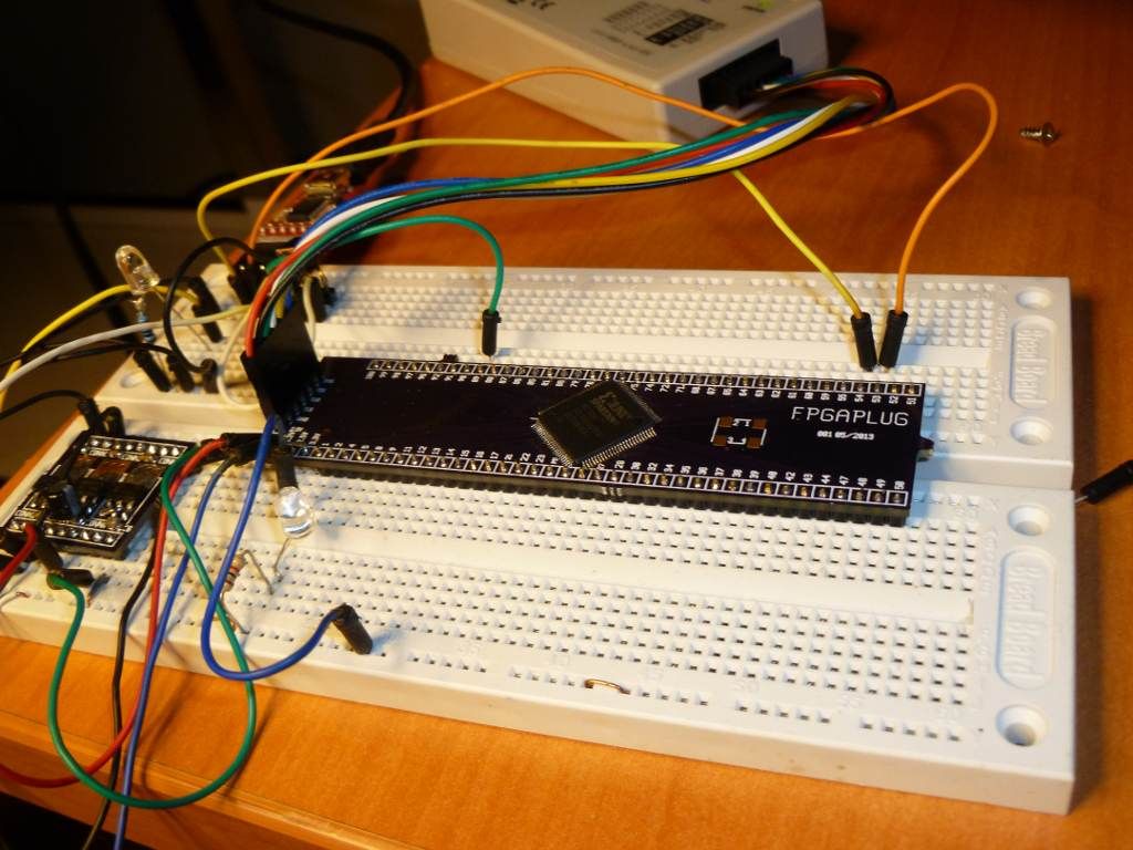
Thus, the Spartan-3 XC3S50A-1VQx100I FPGA is my target. I have several reasons for choosing that FPGA and package. One of them is that the XC3S200A-1VQG100I is a drop-in upgrade. Another is that I wanted to see how much stuff I could fit into the XC3S50A part.
(5) I designed the clock circuitry to use a standard baud rate oscillator.
In the -1 speed grade, the current core will not work at a bus clock rate greater than 16 MHz. A 14.7456 MHz oscillator is the nearest baud rate frequency. With a -2 speed grade, (not available in industrial temp from Digi-Key when I ordered my parts) an 18.432 MHz oscillator will work just fine. The internal frequency of operation is always 4x that provided. Phi1 and Phi2 are essentially the same as the supplied reference clock. There may a phase shift, so I recommend using Phi1 as the reference for any external UARTs that you may decide to attach to the M65C02.
(6) I have not attempted to implement the nSO pin or function.
This may be of use in some applications, but I believe that the nNMI and nIRQ pins and functions, along with the BRK instruction, should suffice for most applications. I believe that I have implemented the WAI instruction correctly, and also the nVP pin and function. Altogether, the M65C02 should be capable of emulating the external interface of a 6502-compatible processor in a sufficiently accurate manner that you should be able execute most existing code.
(7) The memory interface supports asynchronous SRAMs and EPROMs.
Separate read enable and write strobes are provided. I believe that the basic memory cycle that I've built into the M65C02 will let you easily use low-cost 10-12ns asynchronous SRAMs (0 wait state), and low-cost 70 ns asynchronous Flash EPROMs (1 wait state). I've also used all three of the Block RAMs that are available in the XC3S50A part. Two are used for the microprogram, and 1 is used as a 2kx8 Boot ROM.
An external input pin can be used to write protect the vector area. An on-chip PU enables writes to the 2kx8 Boot ROM so both the ROM and the vectors can be changed by software/firmware.
If these restrictions/limitations are acceptable, then I would be glad for you to use the M65C02 processor implementation that I posted. I will provide as much help as I can given my current schedule and time commitments. If it would help, I would be happy to send you (via PM) a ZIP of the ISE 10.1i project that I used to develop the M65C02. I am confident that the behavioral simulation I have performed has fully tested the design, and it should be fairly simple to bring it up on your prototype HW.
|
