Summary: I present the design and implementation details for what may be the most inexpensive and minimal FPGA board. The board is capable of hosting Arlet's core with 8K of RAM/ROM running at 100MHz, glue logic and custom IO. I will update this top page with the most current information as needed.
Attachment:
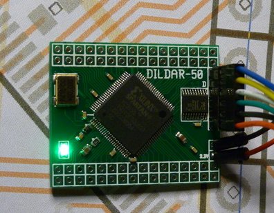 Image1.JPG [ 38.77 KiB | Viewed 1922 times ]
Features-Fast Xilinx XC3S50 FPGA (grade 5), 768 slices, 8K BRAM
-60MHz oscillator (other frequencies can be derived easily)
-Onboard power regulators (1.2V and 2.5V)
-Xilinx Platform Flash
-Native JTAG connection to both FPGA and Platform Flash
-60 IO pins connected (2 are limited: oscillator input and LED output)
-3.3V operation, 5V tolerant (according to information available, not tested)
-IO pin layout allows breadboarding, PCB or wire wrapping
Possible uses-Stand-alone 6502 controller (like arduino but with a 100MHz 6502!)
-A controller with up to 4 PicoBlaze processors
-Glue logic for 6502 (or any) project
-Custom circuitry and interface (keyboard, mouse, VGA, SD card, etc)
-Anything you can imagine
MotivationEvery now and then I wish I had a truly inexpensive FPGA-based controller with a few dozen IO pins. The devboards out there are generally over $100. Devboards stop being available as soon as a new FPGA generation comes out.
Devboards are generally not minimal, and are often built to showcase some or other technology. I could not find a truly minimal board. Boards like Xula have no native JTAG, not minimal (due to the PIC chip) and require yet another set of tools to configure.
Development statusAug 18 2013 - The board is in its 5th revision (E) and is stable and as far as I know is bug-free.
AvailabilitySmall quantities of assembled boards are available on experimental basis to 6502.org members for US$20 plus shipping (for now).
PM me if you are interested in assembled boards, parts or bare PCBs.Working with DILDARThe board is a plain-vanilla FPGA with a JTAG interface, so there is nothing special about using it. Any circuit that fits the XC3S50 should work.
Intellectual PropertyUnless otherwise noted, all information presented here is placed into the Public Domain where it is legally acceptable. I don't care much for the IP situation; the design is a straightforward and commonsense implementation of publicly available information, and I do not believe that anyone (myself included) could have any IP claims. Any designs, software or physical hardware you may get from me should be considered experimental, as is, and not used for any important purpose.
I've also created a version of this board with a 128K SRAM chip.
http://forum.6502.org/viewtopic.php?f=10&t=2644


