This is what I had previously. I thought it would be cool to show the full code and some pics.
Code:
/*
* top level module
*
* (C) Arlet Ottens <arlet@c-scape.nl>
*
*/
module main(
input clk100,
input [15:0] SRD, //SyncRAM data
output pclk_out,
output SRCLK, //SyncRAM clock
output [4:0] red,
output [5:0] green,
output [4:0] blue,
output vsync,
output hsync,
output reg DACBLANKn = 1,
output reg SRCS = 1, //SyncRAM CS, active high
output reg WEn = 1, //SyncRAM WE, active low
output reg [20:0] SRA //SyncRAM Address
);
wire [15:0] rgb;
assign blue = rgb[4:0];
assign green = rgb[10:5];
assign red = rgb[15:11];
wire fifo_write;
wire fifo_full;
reg [15:0] fifo_data;
wire pclk0;
wire vtrigger;
/* pixel clock output using DDR flipflop */
ODDR2 ODDRA (
.Q(pclk_out),
.C0(pclk),
.C1(~pclk),
.CE(1'b1),
.D0(1'b1),
.D1(1'b0),
.R(1'b0),
.S(1'b0)
);
/* SyncRAM Clock output also using DDR flipflop */
ODDR2 ODDRB (
.Q(SRCLK),
.C0(pclk),
.C1(~pclk),
.CE(1'b1),
.D0(1'b1),
.D1(1'b0),
.R(1'b0),
.S(1'b0)
);
wire dcm_clk100;
wire clk;
/* clock buffers */
IBUFG IBUFG_clk( .I(clk100), .O(dcm_clk100) );
BUFG BUFG_clk( .I(dcm_clk100), .O(clk) );
BUFG BUFG_PCLK( .I(pclk0), .O(pclk) );
/* Use DCM to generate 25 MHz VGA pixel clock from 100 MHz main clock */
DCM_SP #(
.CLKDV_DIVIDE(4.0),
.CLKFX_DIVIDE(8),
.CLKFX_MULTIPLY(2),
.CLKIN_DIVIDE_BY_2("FALSE"),
.CLKIN_PERIOD(10.0),
.CLKOUT_PHASE_SHIFT("FIXED"),
.CLK_FEEDBACK("1X"),
.DESKEW_ADJUST("SYSTEM_SYNCHRONOUS"),
.DLL_FREQUENCY_MODE("LOW"),
.DUTY_CYCLE_CORRECTION("TRUE"),
.PHASE_SHIFT(0),
.STARTUP_WAIT("FALSE")
) DCM_SP_inst (
.CLKFX(pclk0), // 0 degree DCM CLK output
.CLKFB(pclk), // DCM clock feedback
.PSEN(1'b0), // no variable phase shift
.CLKIN(dcm_clk100), // Clock input (from IBUFG, BUFG or DCM)
.RST(1'b0)
);
/*
* VGA generator
*/
vga vga(
.clk(clk),
.pclk(pclk),
.hsync(hsync),
.vsync(vsync),
.fifo_data(fifo_data),
.fifo_write(fifo_write),
.fifo_full(fifo_full),
.rgb(rgb) ,
.vtrigger(vtrigger)
);
/*
* when vtrigger is pulsed, generate new frame by sending 640x480 pixels
* to FIFO.
*/
reg [11:0] x = 0;
reg [10:0] y = 0;
wire xdone = (x == 639) && !fifo_full;
wire ydone = (y == 480);
/*
* count x, reset at end of line, and pause when FIFO is full
*/
always @(posedge clk)
if( vtrigger || xdone )
x <= 0;
else if( !fifo_full )
x <= x + 1;
/*
* count y, reset at start of new frame, and increment at end
* of line. Pause when FIFO is full.
*/
always @(posedge clk)
if( vtrigger )
y <= 0;
else if( xdone && !ydone )
y <= y + 1;
/*
* only write fifo during active pixels
*/
assign fifo_write = !ydone;
/*
* SyncRAM address generator
*/
parameter a=3,
b=4; //block size
always @(posedge clk)
if( vtrigger )
SRA <= 0;
else if ( !fifo_full & (x[b] ^ y[b]) )
SRA <= SRA + 1;
/*
* demo test output using external SyncRAM input
*/
always @*
if( y < 1 || y > 479 || x < 1 || x > 639 )
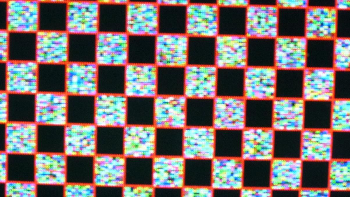
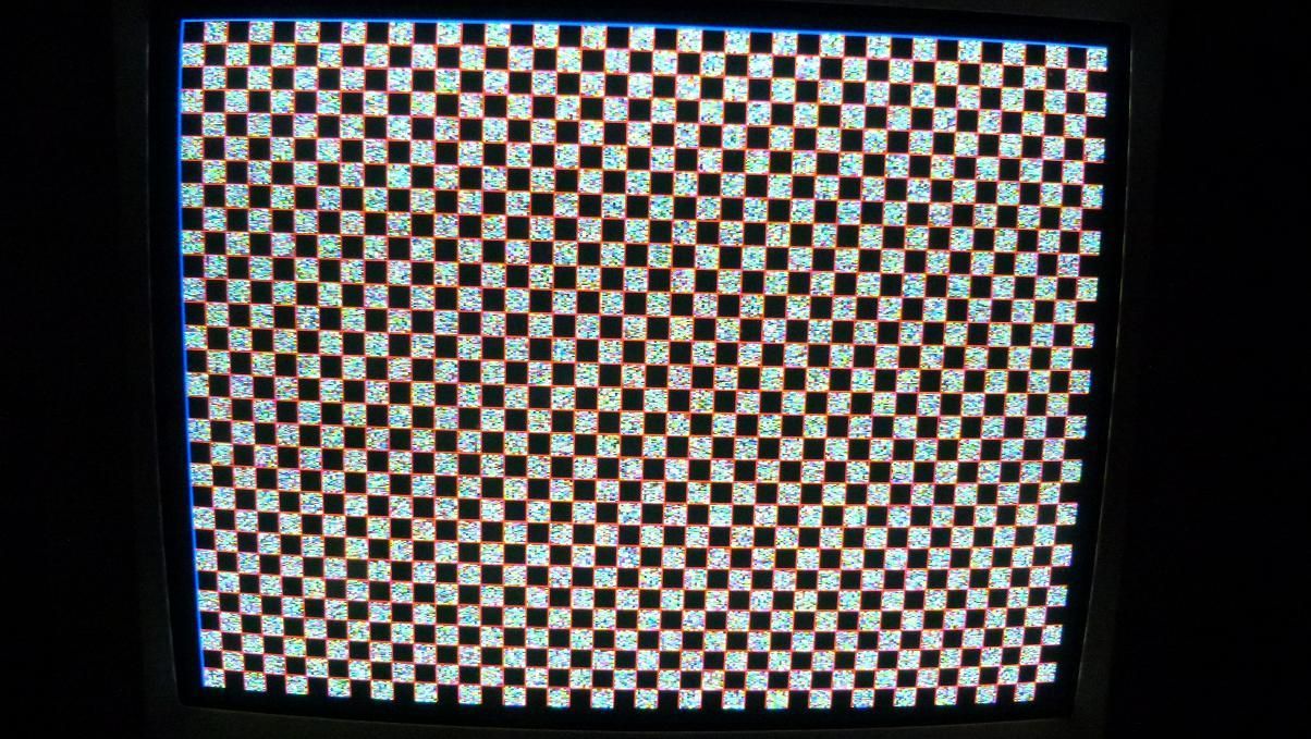
fifo_data = 16'b00000_000000_11111; // blue border
else if( x[a:0] == 0 || y[a:0] == 0 )
fifo_data = 16'b11111_000000_00000; // red lines
else if( x[b] ^ y[b] )
fifo_data = SRD; // RAM data
else
fifo_data = 16'b00000_000000_00000; // black squares
endmodule
CLOSE-UP - (Sorry about the focus):