I must confess it has taken me a few weeks after coming up with this idea of parallel computing, even after 99% completion of board design, to wrap my little mind around this design. It is not a simple one. I will tell you all honestly, what gives me confidence is that Arlet has agreed to help develop the HDL for this project. He has shown great skill in the recent past developing
sprites with SDRAM timing for
v1.1 of the 65Org16 devboard. But this design is totally separate from that one and I'm not calling this project a devboard. Hopefully, some of his hard work will be able to be imported into this design. I believe it will be... My intent here is to concentrate more on the video aspect and change to a more common VGA DB-15 style video output, while maintaining a 3.8"x2.5" board space...
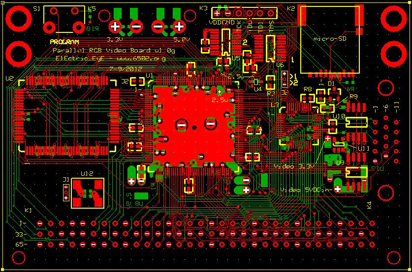
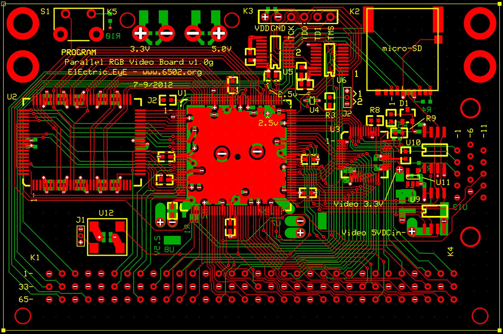
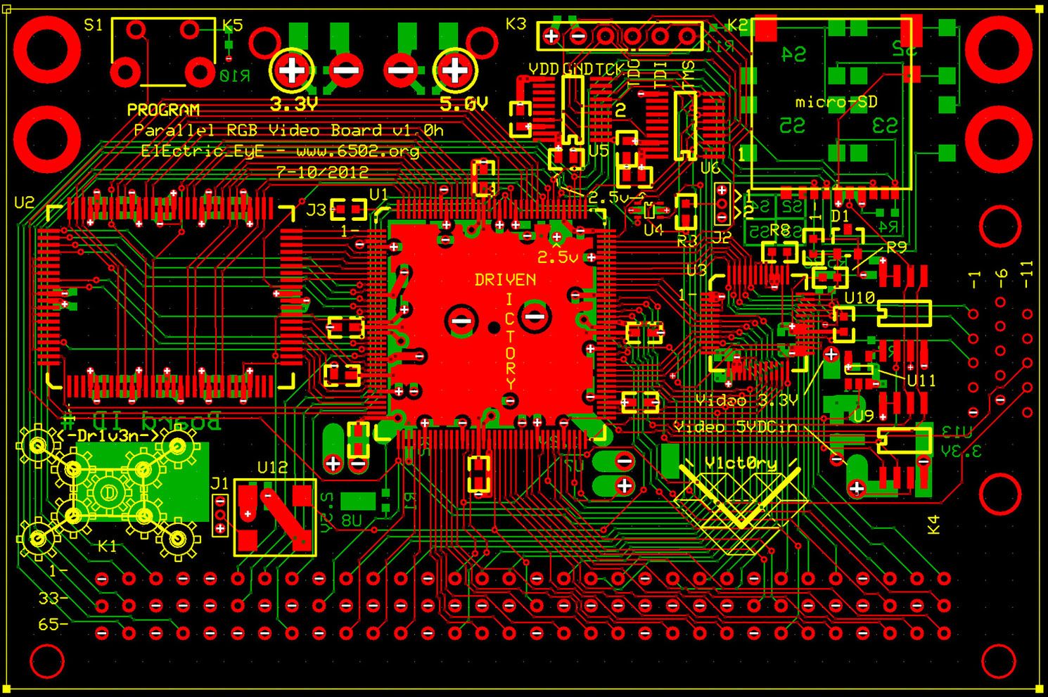
This is the board layout, as it is now. Complete, unless a suggestion is made to improve it in some way. In another
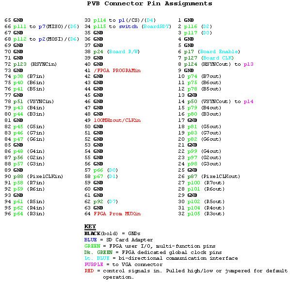
thread some people like Garth and Arlet have made important suggestions that I've taken into consideration for the layout of this board. Garth made suggestions regarding the main 96-pin connector GND layout and Arlet suggested a micro-SD card connector and also important suggestions regarding high frequency noise filtering for the videoDAC power supply. Also BigEd encouraged me to continue on a path of mixing video digitally when I started to stray into analog... Thanks all!
Link to
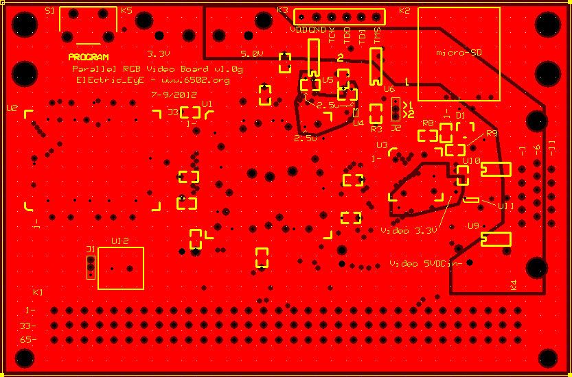
CLOSEUP of layout for v1.0g: Original version.
Link to
CLOSEUP of layout for v1.0h: Fixed layout errors with U4 MUX. Deleted FPGA control of DACBLANKn. Added FPGA control of SyncRAM ADV/LOADn pin. Also, added 4 momentary push-button switches for debugging/control purposes.
Let me try to explain the
concept of the 16-bit design: Each video board has a 2MBx18 synchronous pass-through RAM (16-bits are used for 5-6-5 RGB, 2 parity bits unused...), a 144-pin Spartan 6, a videoDAC, a 3-row 96-pin main connector, and a DB-15 VGA connector for a monitor. The 96-pin main connector allows 16-bit RGB data in, HSYNCin, VSYNCin and PixelClockIn. These signals originate from another video boards' 16-bit RGB data out, HSYNCout, VSYNCout, PixelClockout and are also present on the main connector. The next video board in line can add depth to the video being displayed. Depending on the math, many possibilities exist... It'll be interesting to see how many boards can be successfully cascaded. For now, 4 can fit on another 'in situ'
mainboard. We should be able to do preliminary tests in order to verify the design actually works using just 1 standalone video board without the need for a mainboard and controller board.
Looking at the board layout above, I will explain the
design starting with U12. A 100MHz (200MHz alt.) oscillator goes to 2 global clocks on 2 separate IOBs on the FPGA, it is expected to divide this clock internally for less jitter. It also goes offboard through the main connector. A jumper (J1) can disable this clock and make its output high impedance. This jumper allows for an outside clock to synchronize multiple boards.
U2 is the 6.5ns pass-through synchronous RAM. 16bits of the databus go to the 4th IOB, top of the S6 (U1). All address lines go to the 1st IOB on the left of the S6. The remaining SyncRAM signals connected to FPGA global clocks are: the main CLK, R/W and ChipSelect.
U5 & U6 are basically 2 XCF04S FPGA PROMs connected in parallel, with standard JTAG connections. iMPACT should be able to see both and either can be programmed. Their serial outputs are multiplexed by U4 (a tinylogic '157 2:1 MUX). It's output goes to the FPGA. The MUX control is a jumpered (J2) resistor (R3), in order to be a pull-up or pull-down. This MUX control also receives a signal from offboard allowing for remote control, hence the resistor. The FPGA /Program signal is also routed offboard. There is also a push button(S1) for manual /Program control.
U9 & U10 are 64Mbit SPI serial FLASH. They each have common dedicated SPI lines, meaning only 1 can be selected at any time. This is done from a S6 /CS signal and U9 inverter.
U3 is the videoDAC. 16 signals for 5-6-5 RGB come from IOB3. The video DAC clock and blank signals come from FPGA global clock pins.
The micro-SD adapter has a built in switch when a card is present. This switch signal is present to the S6, letting it know when to use SPI communications. This signal is also output through the main connector (pin34), consider it a "Board Ready" signal. The SPI clk input is common to the one used for the serial FLASHs. If no card is present, MISO, MOSI, and CE (of the SD-Card adapter) are instead used as additional signals for an 8-bit parallel interface to control the video board via remote commands. This interface consists of 8 bi-directional data bus, R/W, Board Select and Board Ready previously mentioned. The Board CLK input signal is also present to a globalclock and orignates from a Controller Board. Specifications will need to be hashed out for commands to/from this interface, but these pins are there for development.
Constraints file:
Code:
# Main Clocks & SPI FLASH Clk #
NET "MAINCLK1" LOC = P55 | IOSTANDARD = LVCMOS33; //N_GCLK
NET "MAINCLK1" TNM_NET = "MAINCLK1";
TIMESPEC TS_MAINCLK1 = PERIOD "MAINCLK1" 10 ns HIGH 50 %;
//NET "MAINCLK2" LOC = P84 | IOSTANDARD = LVCMOS33; //N_GCLK
//NET "MAINCLK2" TNM_NET = "MAINCLK2";
//TIMESPEC TS_MAINCLK2 = PERIOD "MAINCLK2" 10 ns HIGH 50 %;
//NET "SCK" LOC = P94 | IOSTANDARD = LVCMOS33 | SLEW = SLOW | DRIVE = 12; //P_GCLK
# Synchronous Ram Signals #
//NET "SRA[0]" LOC = P26 | IOSTANDARD = LVCMOS33 | SLEW = SLOW | DRIVE = 12; //USER I/O
//NET "SRA[1]" LOC = P27 | IOSTANDARD = LVCMOS33 | SLEW = SLOW | DRIVE = 12; //USER I/O
//NET "SRA[2]" LOC = P29 | IOSTANDARD = LVCMOS33 | SLEW = SLOW | DRIVE = 12; //USER I/O
//NET "SRA[3]" LOC = P30 | IOSTANDARD = LVCMOS33 | SLEW = SLOW | DRIVE = 12; //USER I/O
//NET "SRA[4]" LOC = P32 | IOSTANDARD = LVCMOS33 | SLEW = SLOW | DRIVE = 12; //USER I/O
//NET "SRA[5]" LOC = P33 | IOSTANDARD = LVCMOS33 | SLEW = SLOW | DRIVE = 12; //USER I/O
//NET "SRA[6]" LOC = P34 | IOSTANDARD = LVCMOS33 | SLEW = SLOW | DRIVE = 12; //VREF
//NET "SRA[7]" LOC = P35 | IOSTANDARD = LVCMOS33 | SLEW = SLOW | DRIVE = 12; //USER I/O
//NET "SRA[8]" LOC = P16 | IOSTANDARD = LVCMOS33 | SLEW = SLOW | DRIVE = 12; //N_GCLK
//NET "SRA[9]" LOC = P15 | IOSTANDARD = LVCMOS33 | SLEW = SLOW | DRIVE = 12; //P_GCLK
//NET "SRA[10]" LOC = P14 | IOSTANDARD = LVCMOS33 | SLEW = SLOW | DRIVE = 12; //N_GCLK
//NET "SRA[11]" LOC = P12 | IOSTANDARD = LVCMOS33 | SLEW = SLOW | DRIVE = 12; //USER I/O
//NET "SRA[12]" LOC = P11 | IOSTANDARD = LVCMOS33 | SLEW = SLOW | DRIVE = 12; //USER I/O
//NET "SRA[13]" LOC = P10 | IOSTANDARD = LVCMOS33 | SLEW = SLOW | DRIVE = 12; //USER I/O
//NET "SRA[14]" LOC = P9 | IOSTANDARD = LVCMOS33 | SLEW = SLOW | DRIVE = 12; //USER I/O
//NET "SRA[15]" LOC = P8 | IOSTANDARD = LVCMOS33 | SLEW = SLOW | DRIVE = 12; //USER I/O
//NET "SRA[16]" LOC = P7 | IOSTANDARD = LVCMOS33 | SLEW = SLOW | DRIVE = 12; //USER I/O
//NET "SRA[17]" LOC = P6 | IOSTANDARD = LVCMOS33 | SLEW = SLOW | DRIVE = 12; //USER I/O
//NET "SRA[18]" LOC = P5 | IOSTANDARD = LVCMOS33 | SLEW = SLOW | DRIVE = 12; //USER I/O
//NET "SRA[19]" LOC = P2 | IOSTANDARD = LVCMOS33 | SLEW = SLOW | DRIVE = 12; //USER I/O
//NET "SRA[20]" LOC = P1 | IOSTANDARD = LVCMOS33 | SLEW = SLOW | DRIVE = 12; //VREF
//NET "SRD[0]" LOC = P121 | IOSTANDARD = LVCMOS33 | SLEW = SLOW | DRIVE = 12; //USER I/O
//NET "SRD[1]" LOC = P126 | IOSTANDARD = LVCMOS33 | SLEW = SLOW | DRIVE = 12; //N_GCLK
//NET "SRD[2]" LOC = P131 | IOSTANDARD = LVCMOS33 | SLEW = SLOW | DRIVE = 12; //N_GCLK
//NET "SRD[3]" LOC = P132 | IOSTANDARD = LVCMOS33 | SLEW = SLOW | DRIVE = 12; //P_GCLK
//NET "SRD[4]" LOC = P134 | IOSTANDARD = LVCMOS33 | SLEW = SLOW | DRIVE = 12; //P_GCLK
//NET "SRD[5]" LOC = P137 | IOSTANDARD = LVCMOS33 | SLEW = SLOW | DRIVE = 12; //USER I/O
//NET "SRD[6]" LOC = P138 | IOSTANDARD = LVCMOS33 | SLEW = SLOW | DRIVE = 12; //USER I/O
//NET "SRD[7]" LOC = P139 | IOSTANDARD = LVCMOS33 | SLEW = SLOW | DRIVE = 12; //USER I/O
//NET "SRD[8]" LOC = P118 | IOSTANDARD = LVCMOS33 | SLEW = SLOW | DRIVE = 12; //USER I/O
//NET "SRD[9]" LOC = P119 | IOSTANDARD = LVCMOS33 | SLEW = SLOW | DRIVE = 12; //USER I/O
//NET "SRD[10]" LOC = P120 | IOSTANDARD = LVCMOS33 | SLEW = SLOW | DRIVE = 12; //VREF
//NET "SRD[11]" LOC = P133 | IOSTANDARD = LVCMOS33 | SLEW = SLOW | DRIVE = 12; //N_GCLK
//NET "SRD[12]" LOC = P140 | IOSTANDARD = LVCMOS33 | SLEW = SLOW | DRIVE = 12; //USER I/O
//NET "SRD[13]" LOC = P141 | IOSTANDARD = LVCMOS33 | SLEW = SLOW | DRIVE = 12; //USER I/O
//NET "SRD[14]" LOC = P142 | IOSTANDARD = LVCMOS33 | SLEW = SLOW | DRIVE = 12; //USER I/O
//NET "SRD[15]" LOC = P143 | IOSTANDARD = LVCMOS33 | SLEW = SLOW | DRIVE = 12; //VREF
//NET "WEn" LOC = P21 | IOSTANDARD = LVCMOS33; //N_GCLK
//NET "SRCLK" LOC = P22 | IOSTANDARD = LVCMOS33; //P_GCLK
//NET "SRCS" LOC = P23 | IOSTANDARD = LVCMOS33; //N_GCLK
# RGBin Signals #
//NET "Rin[0]" LOC = P64 | IOSTANDARD = LVCMOS33; //CSI
//NET "Rin[1]" LOC = P62 | IOSTANDARD = LVCMOS33; //Dx
//NET "Rin[2]" LOC = P61 | IOSTANDARD = LVCMOS33; //Dx
//NET "Rin[3]" LOC = P59 | IOSTANDARD = LVCMOS33; //Dx
//NET "Rin[4]" LOC = P58 | IOSTANDARD = LVCMOS33; //Dx
//NET "Gin[0]" LOC = P57 | IOSTANDARD = LVCMOS33; //Dx
//NET "Gin[1]" LOC = P56 | IOSTANDARD = LVCMOS33; //N_GCLK
//NET "Gin[2]" LOC = P48 | IOSTANDARD = LVCMOS33; //Dx
//NET "Gin[3]" LOC = P47 | IOSTANDARD = LVCMOS33; //RDWR_B_VREF
//NET "Gin[4]" LOC = P46 | IOSTANDARD = LVCMOS33; //Dx
//NET "Gin[5]" LOC = P45 | IOSTANDARD = LVCMOS33; //Dx
//NET "Bin[0]" LOC = P44 | IOSTANDARD = LVCMOS33; //Dx
//NET "Bin[1]" LOC = P43 | IOSTANDARD = LVCMOS33; //Dx
//NET "Bin[2]" LOC = P41 | IOSTANDARD = LVCMOS33; //Dx
//NET "Bin[3]" LOC = P40 | IOSTANDARD = LVCMOS33; //Dx
//NET "Bin[4]" LOC = P38 | IOSTANDARD = LVCMOS33; //CSO
//NET "HSYNCin" LOC = P123 | IOSTANDARD = LVCMOS33; //P_GCLK
//NET "VSYNCin" LOC = P51 | IOSTANDARD = LVCMOS33; //N_GCLK
//NET "PCLKin" LOC = P88 | IOSTANDARD = LVCMOS33; //N_GCLK
# RGBout Signals #
NET "Rout[0]" LOC = P105 | IOSTANDARD = LVCMOS33 | SLEW = SLOW | DRIVE = 12; //USER I/O
NET "Rout[1]" LOC = P104 | IOSTANDARD = LVCMOS33 | SLEW = SLOW | DRIVE = 12; //VREF
NET "Rout[2]" LOC = P102 | IOSTANDARD = LVCMOS33 | SLEW = SLOW | DRIVE = 12; //USER I/O
NET "Rout[3]" LOC = P101 | IOSTANDARD = LVCMOS33 | SLEW = SLOW | DRIVE = 12; //USER I/O
NET "Rout[4]" LOC = P100 | IOSTANDARD = LVCMOS33 | SLEW = SLOW | DRIVE = 12; //USER I/O
NET "Gout[0]" LOC = P99 | IOSTANDARD = LVCMOS33 | SLEW = SLOW | DRIVE = 12; //USER I/O
NET "Gout[1]" LOC = P98 | IOSTANDARD = LVCMOS33 | SLEW = SLOW | DRIVE = 12; //USER I/O
NET "Gout[2]" LOC = P97 | IOSTANDARD = LVCMOS33 | SLEW = SLOW | DRIVE = 12; //USER I/O
NET "Gout[3]" LOC = P83 | IOSTANDARD = LVCMOS33 | SLEW = SLOW | DRIVE = 12; //USER I/O
NET "Gout[4]" LOC = P82 | IOSTANDARD = LVCMOS33 | SLEW = SLOW | DRIVE = 12; //USER I/O
NET "Gout[5]" LOC = P81 | IOSTANDARD = LVCMOS33 | SLEW = SLOW | DRIVE = 12; //USER I/O
NET "Bout[0]" LOC = P80 | IOSTANDARD = LVCMOS33 | SLEW = SLOW | DRIVE = 12; //USER I/O
NET "Bout[1]" LOC = P79 | IOSTANDARD = LVCMOS33 | SLEW = SLOW | DRIVE = 12; //USER I/O
NET "Bout[2]" LOC = P78 | IOSTANDARD = LVCMOS33 | SLEW = SLOW | DRIVE = 12; //USER I/O
NET "Bout[3]" LOC = P75 | IOSTANDARD = LVCMOS33 | SLEW = SLOW | DRIVE = 12; //AWAKE
NET "Bout[4]" LOC = P74 | IOSTANDARD = LVCMOS33 | SLEW = SLOW | DRIVE = 12; //DOUT_BUSY
NET "DACBLANKn" LOC = P85 | IOSTANDARD = LVCMOS33 | SLEW = SLOW | DRIVE = 12; //P_GCLK Alt. v1.0h -> NET "LOADn" LOC = P85 | IOSTANDARD = LVCMOS33 | SLEW = SLOW | DRIVE = 12; //P_GCLK
NET "HSYNCout" LOC = P124 | IOSTANDARD = LVCMOS33 | SLEW = SLOW | DRIVE = 12; //N_GCLK
NET "VSYNCout" LOC = P50 | IOSTANDARD = LVCMOS33 | SLEW = SLOW | DRIVE = 12; //P_GCLK
NET "PCLKout" LOC = P87 | IOSTANDARD = LVCMOS33 | SLEW = SLOW | DRIVE = 12; //P_GCLK
# SD Card and I/O #
//NET "BOARDRDYn" LOC = P115 | IOSTANDARD = LVCMOS33 | SLEW = SLOW | DRIVE = 12; //USER I/O -- Alt. v1.0h S5
//NET "BOARDCLK" LOC = P127 | IOSTANDARD = LVCMOS33; //N_GCLK
//NET "BOARDEN" LOC = P17 | IOSTANDARD = LVCMOS33; //P_GCLK
//NET "BOARDRWn" LOC = P24 | IOSTANDARD = LVCMOS33; //P_GCLK
//NET "IOD[0]" LOC = P66 | IOSTANDARD = LVCMOS33 | SLEW = SLOW | DRIVE = 12; //Dx
//NET "IOD[1]" LOC = P67 | IOSTANDARD = LVCMOS33 | SLEW = SLOW | DRIVE = 12; //Dx
//NET "IOD[2]" LOC = P116 | IOSTANDARD = LVCMOS33 | SLEW = SLOW | DRIVE = 12; //USER I/O
//NET "IOD[3]" LOC = P117 | IOSTANDARD = LVCMOS33 | SLEW = SLOW | DRIVE = 12; //USER I/O
//NET "IOD[4]" LOC = P114 | IOSTANDARD = LVCMOS33 | SLEW = SLOW | DRIVE = 12; //USER I/O -- Alt. MicroSD CSn or v1.0h S3
//NET "IOD[5]" LOC = P111 | IOSTANDARD = LVCMOS33 | SLEW = SLOW | DRIVE = 12; //USER I/O -- Alt. MicroSD MISO or v1.0h S4
//NET "IOD[6]" LOC = P112 | IOSTANDARD = LVCMOS33 | SLEW = SLOW | DRIVE = 12; //USER I/O -- Alt. MicroSD MOSI or v1.0h S2
//NET "IOD[7]" LOC = P92 | IOSTANDARD = LVCMOS33 | SLEW = SLOW | DRIVE = 12; //N_GCLK
# SPI Flash Data #
//NET "SO" LOC = P95 | IOSTANDARD = LVCMOS33 | SLEW = SLOW | DRIVE = 12; //N_GCLK
//NET "SI" LOC = P93 | IOSTANDARD = LVCMOS33; //P_GCLK
//NET "FEN12n" LOC = P72 | IOSTANDARD = LVCMOS33 | SLEW = SLOW | DRIVE = 12; //CMPCS_B_2
The Parts List:
Code:
QTY Price Description Part# Package Supplier ID
-------------------------------------------------------------------------------------------------------------
2 $6.95 FPGA Prom XCF04S 20-pin TSSOP Digi-Key U5,U6
1 $17.22 FPGA XC6SLX9-3TQG144I 144-pin QFP Digi-Key U1
1 $9.24 Video DAC ADV7125KSTZ140-ND 48-pin QFP Digi-Key U3
1 $57.12 2MBx18 SyncRAM 133MHz CY7C1463AV33-133AXC 100-pin QFP Cypress direct U2
1 $160.66 4MBx18 SyncRAM 5.5ns GS8640Z18GT-300I 100-pin QFP Avnet U2 Alt. V1.0h
1 $0.82 TinyLogic 74157 MUX 74AUP1G157 SOT-363 Digi-Key U4
1 $0.49 TinyLogic 7404 Inverter NC7SZ04 SOT-23-5 Digi-Key U11
2 $3.81 64Mb SPI Flash SST25VF064C-80-4I-S3AE 8-pin SOIJ Microchip direct U9,U10
1 $0.74 2.5V 1A VRegulator MCP1826S-2502E/DB-ND SOT-223-3 Digi-Key U8
1 $0.74 1.2V 1A VRegulator MCP1826S-1202E/DB-ND SOT-223-3 Digi-Key U7
1 $0.74 3.3V 1A VRegulator MCP1826S-3302E/DB SOT-223-3 Digi-Key U13
1 $2.41 100MHz 3.3VOsc HCMOS/TTL CTX318LVCT-ND SMD Digi-Key U12
1 $4.64 200MHz 3.3VOsc HCMOS 631-1184-1-ND SMD Digi-Key U12alt
2 $0.84 1ea 22uF 16V X7R cap 445-3955-1-ND 1210 Digi-Key main 3.3V, 5V bypass
2 $0.43 1ea 4.7uF 10V X7R cap 445-1433-1-ND 1210 Digi-Key FPGA 1.2V, 2.5V bypass
30 $0.10 1ea .1uF 25V X7R cap 445-1316-1-ND 0603 Digi-Key
30 $0.10 1ea 10000pF 100V X7R cap 445-1311-1-ND 0603 Digi-Key
1 $0.11 1ea 1uF 15V X7R cap 445-1604-1-ND 0603 Digi-Key
1 $0.40 1ea 10uF 10V X7R cap 445-6857-1-ND 0805 Digi-Key video 3.3V bypass
1 $0.74 10ea 4.7Kohm resistor 541-4.7KGCT-ND 0603 Digi-Key R1,R2,R3,R4,R10
1 $0.74 10ea 75ohm resistor 541-75GCT-ND 0603 Digi-Key R5,R6,R7
1 $0.81 10ea 536ohm resistor 541-536HCT-ND 0603 Digi-Key R8
1 $0.74 10ea 1Kohm resistor 541-1.0KGCT-ND 0603 Digi-Key R9,R11
1 $0.17 1ea 160ohm Ferrite bead 240-2411-1-ND 1206 Digi-Key L1
1 $1.92 1ea Zener Diode AD1580ARTZ-REEL7CT-ND SOT-23 Digi-Key D1
1 $1.62 4-pin .2" male Molex WM6988-ND r. angle thru-hole Digi-Key K5
1 $0.63 6-pin .1" male SIP A1918-ND r. angle thru-hole Digi-Key K3
1 $1.96 Micro-SD adapter HR1964CT-ND SMD Digi-Key K2
1 $1.41 VGA connector (blue) A35119-ND r. angle thru-hole Digi-Key K4
1 $4.85 96-pin male receptacle A32857-ND vertical thru-hole Digi-Key K1receptacle
1 $5.43 96-pin female plug A32863-ND r. angle thru-hole Digi-Key K1
10 $0.20 .050" jumper S9014E-03-ND thru-hole Digi-Key J1,J2
10 $0.24 .050" jumper short S9345-ND Digi-Key
1 $0.35 Momentary switch P12233SCT-ND r. angle thru-hole Digi-Key S1
1 $0.69 mom push switch yellow SW416-ND SMD Digi-Key S2,S3,S4,S5 (v1.0h)
Observations: I think we will need very quick parallel 6-bit ALUs that can do add, subtract, logic AND, OR, EOR, no carry needed on a pixel clock to each Red Green Blue databus to the videoDAC. Once the first board does this math/logical operation in as few cycles as possible, it passes the HSYNC,VSYNC, PixelClock, and 16-bit RGB data into the following 'parallel' board.
Recognize that the following board does not read this data and put it into it's own RAM. It is the programmers responsibility to program into the videoRAM of each board what each board is meant to output for the total summation effect. But more on the internals later, it still scrambles my mind!. This is Arlet's speciality. But I do intend to continue my learning some Verilog from this project, so be warned of stupid questions!
--------------------------------------------------------------------------------------------------------------------------------------------------------------------------------------------
EDIT: 11/7/2013-... In an
attempt to categorize parts of this thread, which has become quite long to some members' chagrin but was not my intention, I will post a 'concentrated minutes' for each page. This will consist of 1 or 2 sentences.
Page 1: Discussions regarding the concept. Simultaneously Switching Output (SSO) problem of FPGAs. HDMI output? Layout and main connector almost done. IO communication dicussion.
Page 2: More discussions on IO. Realization of a backplane design in order to solidify signals on each PVB. Use of GCLKs in FPGA.
Page 3: SyncRAM chosen, parts list completed. First board design .g manufacture order placed. Problems realized. Parts ordered to complete 1 PVB. Version .h started.
Page 4: Pic for tools I used for construct. Closeup of 1.0g board front and back. Pic's of soldering attempts. Initial testing of FPGA and 2xPROMs successful. HSYNC & VSYNC signals successful in Verilog (started Implementation thread). Found faster SyncRAM.
Page 5: Loftier goals of 1900x1080... Arlet adds RDY signal to his core. More PVB version .h info.
Page 6: Version 1.0h boards received. No schematics? Info of new GSI SyncRAM's. Arlet receives a V1.0h 'bare' board. A
new thread is started (nov 9th - dec 1st) to try to draw lines in hardware. Arlet "races the beam".
Page 7: My first attempt at drawing a line in hardware, confirmed on the board Arlet received. He begins to write his own code: An improved VGA timing generator, a FIFO buffer and more...
This page is worth reading.Page 8: External memory controllers. Some of Arlet's code modified and some pics... Talk of delaying input signals going through IOB's.
Page 9: Experimenting with Verilog syntax. Arlet's board experiences an unknown problem.
Page 10: Questions about the PVB v.10h construction.
Page 11; Arlet fixes the problem with his board. Issue that caused problem remains unsolved but his board works again. More of Arlet's hardware line generator.
Page 12: More hardware lines in Verilog.
Page 13: Block diagram of the 65Org16 system on paper. Starting to learn Verilog by building a SoC on FPGA.
Page 14: Setting up the blockRAMs, initializing BRAMs. wired OR vs. internal tri-states for databuses. Using Arlet's .coe generator for initializing BRAMs.
Page 15: Arlet's makes bin2hex! Bringing up the simple SoC. Finding errors...
Page 16: Michael finds error in the .coe file. Also reverted back to older version 65Org16.b core. Signs of life of cpu writing to video SyncRAM and visible video output. Youtube video.
Page 17: Experimentation with different system speeds
writing to SyncRAM only, and different resolutions begin. Porting over software, from old TFT project, to plot character bitmaps. Noise issues, experimentation with FPGA pin DRIVE strength to resolve.
Page 18: Talk of Arlet's 6502 Sandbox board and bypassing, some pics. More talk of bypass cap values. Garth has great links for design engineers and bypass cap's. Trying IOBDELAY again.
Page 19: Arlet has great ideas for video memory mapping in the 65Org16 64Kx16 zero page. I
begin to understand his 'indirect indexed y' suggestion for memory map interface to the videoRAM. I begin to try to implement it in a clear screen routine.
Page 20: Some talk of Bruces' implemetation of Bob Bishops' Mandelbrot, blitters. Arlet has another idea to map the videospace into 65Org16 64Kx16 zeropage, but only 1 line using different 6502 (abs,x) addressing. The clearscreen routine works using Arlet's 'indirect indexed y' memory map interface.
Page 21: 65Org16.b Clearcreen software posted. Begin plotting pixels in software. Jumping right into plotting circles using software SQUARE and SQUAREROOT sub-routines. 8bit shares his Bresenham Circle 6502 code, losing these routines.
Page 22: Talk of filled circles. Trying to do filled by decreasing radii in concentric circles, also drawing lines in radar sweep. Both unsuccessful as error is seen. 8bit shares his Bresenham line 6502 software. Added a Random Number Generator for plotting and color lookup table. Added an opcode cycle counter that can be read by the 65Org16.
Page 23: Plotting characters using the cpu and the value read from the cycle counter. Barrel shift problem noted in all versions of the
65Org16 ALU when using LSR.
A proper fix to the 65Org16 ALU is on this page. Page 24: Calibrating the opcode cycle counter. Cycle counting some 65Org16.b circle and character plotting routines. Trying to optimize the software.
Page 25: Initial converting of 8bit's 65C02 Bresenham Circle to 65Org16.b assembly and plotting results. Some more problems with the 65Org16.b core. Daryl helps out. A major problem found in the .b core... Software circle plotting works!
Page 26:
EDIT: 8/8/12 - Added detail.
EDIT: 8/8/12 - Added Constraints file.
EDIT: 8/8/12 - Switched SO & FEN12n in Constraint file, updated layout pic.
EDIT: 8/8/12 - Added detail.
EDIT: 8/8/12 - Added more detail.
EDIT: 8/10/12 - Changed Title from Concept Design & Implementation...
EDIT: 8/13/12 - Added Power Plane pic
EDIT: 8/18/12 - Edited Constraints file
EDIT: 8/18/12 - Corrected .UCF file
EDIT: 8/20/12 - Added CLOSEUP link
EDIT: 8/21/12 - A few of last layout/main connector pinout/constraint optimizations
EDIT: 8/22/12 - Parts list additions
EDIT: 8/24/12 - Clarified info regarding Main Board
EDIT: 8/27/12 - Updated Parts List
EDIT: 8/28/12 - Finished Parts List
EDIT: 8/28/12 - Re-clarified old details in order to update design changes
EDIT: 9/3/12 - Added power connector, updated parts list
EDIT: 9/6/12 - Ordered parts today. Updated prices on Parts List. All IC's are up to date as of this EDIT date. Some discrete components are actually cheaper than listed here.
EDIT: 9/23/12 - Corrected .UCF file. Functional.
EDIT: 9/23/12 - Found mixed pins assignments in .UCF file
EDIT: 10/9/12 - Updated .UCF file and parts for v1.0h
EDIT: 10/10/12 - Added link for closeup of v1.0h layout
EDIT: 10/18/12 - Clarified that this is a 3.3V design in the Title
EDIT: 6/11/13 - Added pic of .h board
EDIT: 8/6/13 - Corrected .UCF file for v1.0h, and v1.0h brief
EDIT: 12/7/14 - Added System Block Diagram


