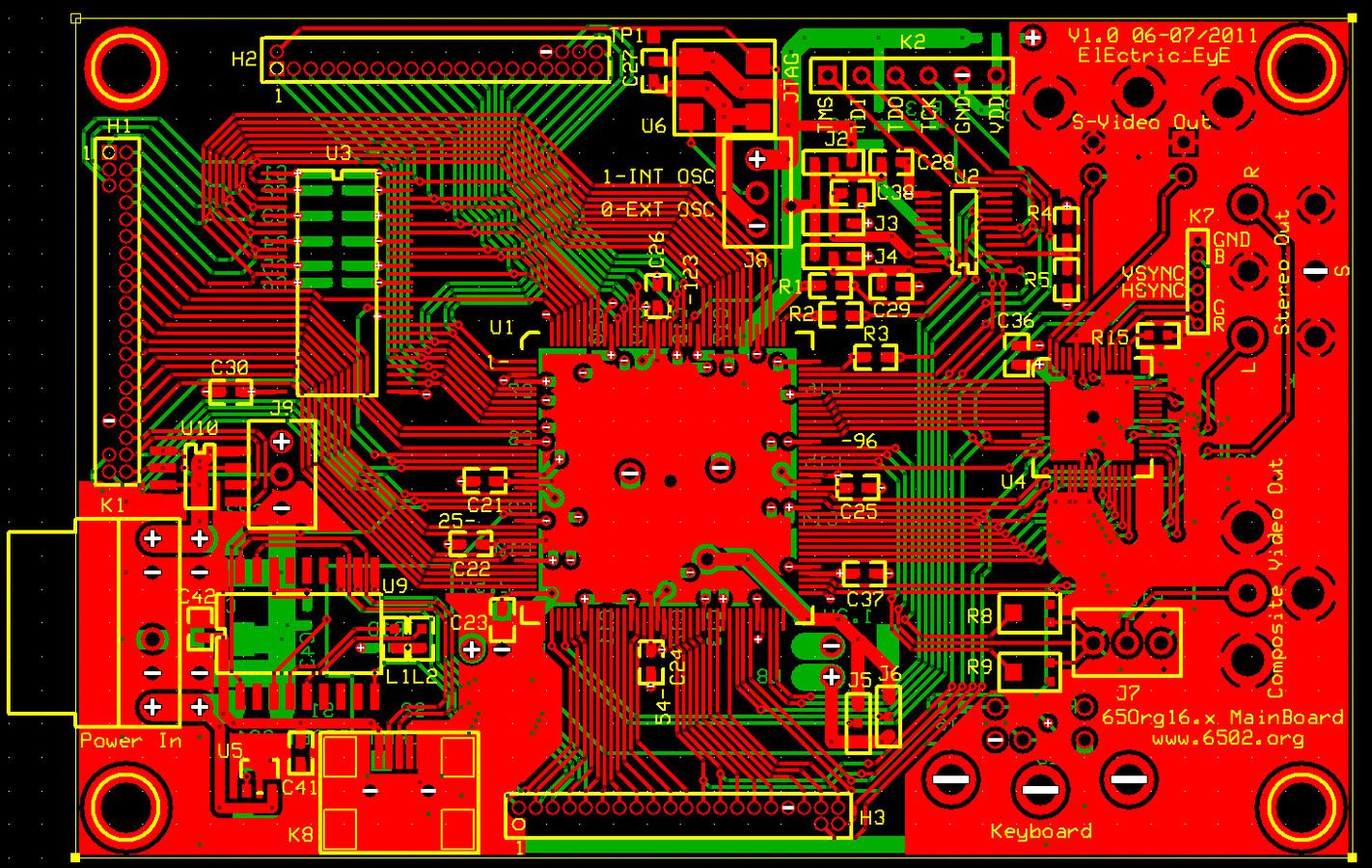
6502.org Forum  Projects  Code  Documents  Tools  Forum
It is currently Mon Apr 29, 2024 4:23 pm

All times are UTC


Post new topic Reply to topic  [ 241 posts ]  Go to page Previous  1, 2, 3, 4, 5, 6, 7, 8 ... 17  Next
Author Message
 Post subject:
PostPosted: Tue Jun 14, 2011 7:24 pm 
Offline

Joined: Mon Mar 02, 2009 7:27 pm
Posts: 3258
Location: NC, USA
OK, sorry. After reading the electrical spec's, ones I usually hunt for after reading the intro, this TI chip is 5V only! I should have realized that from the 1998 date on the datasheet. Lower voltages were not favored back then...

I'll start the schematic tomorrow. Sounds like we're in agreement now for the basic construct.
Too bad there's no other input from the peanut gallery. All comments/suggestions welcome! This 65Org16 mainboard is solidifying...


Last edited by ElEctric_EyE on Mon Nov 21, 2011 9:56 pm, edited 2 times in total.

Top
 Profile  
Reply with quote  
 Post subject:
PostPosted: Wed Jun 15, 2011 4:25 pm 
Offline

Joined: Mon Mar 02, 2009 7:27 pm
Posts: 3258
Location: NC, USA
Laying out the board is very time consuming! Just spent 5 hours on what you see below. I should progress faster though.

So far the Spartan 6, SDRAM, and oscillator have 0603 bypass cap's (will be ceramic types). I plan to superglue the cap's since they're so small, then solder them. I'll attempt wiring up VCCInt and VCCAux next, but I need to get a few chores done...

The 14-pin DIP is a machine tool socket, that will fit either a 1/2size or a full size can oscillator. There is also a jumper to disable or tristate some oscillators (which I realize just now is stupid because you can just remove the oscillator), so the signal can come from offboard. I still have ALOT of work to do, but I figured I would post in case anyone has suggestions or things to be wary of when using ExpressPCB's software.

Critique's welcome please!

Main board layout

EDIT: 14-pin DIP not 8-pin DIP


Last edited by ElEctric_EyE on Mon Nov 21, 2011 9:57 pm, edited 4 times in total.

Top
 Profile  
Reply with quote  
 Post subject:
PostPosted: Wed Jun 15, 2011 6:19 pm 
Offline
User avatar

Joined: Tue Nov 16, 2010 8:00 am
Posts: 2353
Location: Gouda, The Netherlands
ElEctric_EyE wrote:
The 8-pin DIP is a machine tool socket, that will fit either a 1/2size or a full size can oscillator.


How about a small SMD oscillator instead ? You can still multiply/divide the frequency inside the Spartan-6 if you want.


Top
 Profile  
Reply with quote  
 Post subject:
PostPosted: Wed Jun 15, 2011 7:43 pm 
Offline

Joined: Mon Mar 02, 2009 7:27 pm
Posts: 3258
Location: NC, USA
Arlet wrote:
...How about a small SMD oscillator instead ? You can still multiply/divide the frequency inside the Spartan-6 if you want.

Since things are headed towards SMT and they're cheap, I'm inclined to agree although some are BGA style. Which part # were you thinking of?

I've discovered a technique that I'm about to use and update on the Main board layout. I learned it from this video. It will solve many issues. Check it out soon!


Last edited by ElEctric_EyE on Mon Nov 21, 2011 9:59 pm, edited 2 times in total.

Top
 Profile  
Reply with quote  
 Post subject:
PostPosted: Wed Jun 15, 2011 8:31 pm 
Offline
User avatar

Joined: Tue Nov 16, 2010 8:00 am
Posts: 2353
Location: Gouda, The Netherlands
The 7x5 mm oscillators are common and cheap. For example Digi-key part # 887-1185-1-ND, but I just picked the 50 MHz version for no particular reason. They also have smaller ones.


Top
 Profile  
Reply with quote  
 Post subject:
PostPosted: Wed Jun 15, 2011 9:16 pm 
Online
User avatar

Joined: Fri Dec 11, 2009 3:50 pm
Posts: 3349
Location: Ontario, Canada
ElEctric_EyE wrote:
Too bad there's no other input from the peanut gallery. All comments/suggestions welcome!

LOL! Wow, EE -- that's a wide-open invitation! But I do have a few modest suggestions. Hope they're not too (pea-) nutty for ya... :roll:

I guess saving space is a prime priority, so have you considered mounting the voltage regulator vertically? Laying it flat on the board consumes more area, and it probably isn't necessary unless it's a thermal consideration -- ie, you want contact with the board so it'll help cool the reg. Another option (somewhat sloppy) would be to locate at the perimeter and let the reg hang off the edge of the board.

Also, perhaps there's an angle that'd let you locate one or more components on the back of the board -- perhaps even directly opposite the Spartan 6. A simple part like the oscillator would be one possible candidate. You would need a SMD socket. But even the SRAM chip could go there, assuming you're willing to rework the placement of bypass cap's and power connections. As for the signal lines between the Spartan and the SRAM, they'd probably work out beautifully -- very compact & short!

Just beware of mistakes that arise due to the mirror image you're dealing with when components are upside down. ExpessPCB won't help you much with this (although you could define some custom, mirrored components).

cheers,

Jeff


Top
 Profile  
Reply with quote  
 Post subject:
PostPosted: Wed Jun 15, 2011 10:59 pm 
Offline

Joined: Mon Mar 02, 2009 7:27 pm
Posts: 3258
Location: NC, USA
Arlet wrote:
The 7x5 mm oscillators are common and cheap. For example Digi-key part # 887-1185-1-ND, but I just picked the 50 MHz version for no particular reason. They also have smaller ones.

Those were the BGA types I was talking about. Looking at it closer though I see that it may be solderable by hand. I can make a jumper based on 1 of 2 positions. It can select between the onboard SMD output or 1 of the 2 onboard socketed can oscillators. Selecting 1 (either SMD or 1 of the can's) will disable the other to lower noise and power consumption. And if the user doesn't like either one, just unplug the can oscillator, set the jumper to select the can oscillator and feed your offboard signal to pin 8 or pin 11 of the machine tooled socket. I'm still working on the I/O connectors. They will most assuredly come last, as I am still looking for a viable connector style.

Dr Jefyll wrote:
... Wow, EE -- that's a wide-open invitation! But I do have a few modest suggestions. Hope they're not too (pea-) nutty for ya... ... Jeff

Hi Dr. Jeff, nothing is out of the realm of possibility. I consider all options, and thanks for contributing!.
Dr Jefyll wrote:
...I guess saving space is a prime priority, so have you considered mounting the voltage regulator vertically? Laying it flat on the board consumes more area, and it probably isn't necessary unless it's a thermal consideration -- ie, you want contact with the board so it'll help cool the reg. Another option (somewhat sloppy) would be to locate at the perimeter and let the reg hang off the edge of the board...

Well, saving space was a priority when I was trying to stuff the board and do an initial layout with multiple SDRAMs.
I have laid the MCP1826 3.3V Reg flat because when it comes time, it will need to be inside an encloser and vertical space will be limited. I plan to mount it to the board through a space saving horizontally mounted TO-220-3 heat sink. Should be on my [url=http://i207.photobucket.com/albums/bb73/ultimateroadwarrior/Partslist.jpgupdated part's list[/url].
Dr Jefyll wrote:
...Also, perhaps there's an angle that'd let you locate one or more components on the back of the board -- perhaps even directly opposite the Spartan 6...Jeff

The mainboard wasn't updated when you saw it earlier today, I was still updating the design, so you didn't know what I had in mind. I wanted to have all bypass cap's within the circumference underneath the Spartan 6' pins on the opposite side of the board, similar to Intel processor's nowadays (not sure if they're bypass caps underneath the Intel CPU's, but they look like it and thus gave me the idea I've implemented here). But I have updated the Main board design. And I am very happy with it. Extreme attention to detail I have paid to it!

I still need to figure out the bypassing for the 5 Spartan 6 VCCInt pins connected to the big red 1.2V VCCInt power plane. I may just use 1 cap for all 5...

Whew, time for rest.

Time to read [url=http://www.xilinx.com/support/documentation/user_guides/ug393.pdf]UG393[/url]. I meant to read it this morning, but I wanted to dive in and start designing by applying noise reduction techniques I have learned through my wirewrap prototyping...
Time to see where I've gone wrong... or right.


Last edited by ElEctric_EyE on Mon Nov 21, 2011 10:01 pm, edited 2 times in total.

Top
 Profile  
Reply with quote  
 Post subject:
PostPosted: Thu Jun 16, 2011 4:47 am 
Offline
User avatar

Joined: Tue Nov 16, 2010 8:00 am
Posts: 2353
Location: Gouda, The Netherlands
ElEctric_EyE wrote:
Arlet wrote:
The 7x5 mm oscillators are common and cheap. For example Digi-key part # 887-1185-1-ND, but I just picked the 50 MHz version for no particular reason. They also have smaller ones.

Those were the BGA types I was talking about. Looking at it closer though I see that it may be solderable by hand. I can make a jumper based on 1 of 2 positions. It can select between the onboard SMD output or 1 of the 2 onboard socketed can oscillators. Selecting 1 (either SMD or 1 of the can's) will disable the other to lower noise and power consumption.


I solder these by hand all the time. It's really easy, since the pads are fairly big, and you can reach them from the side. The solder will just wick right under the part. If you can solder 0603 by hand, these won't be a problem.


Top
 Profile  
Reply with quote  
 Post subject:
PostPosted: Thu Jun 16, 2011 12:21 pm 
Offline
User avatar

Joined: Fri Aug 30, 2002 9:02 pm
Posts: 1681
Location: Sacramento, CA
ElEctric_EyE wrote:
I've discovered a technique that I'm about to use and update on the Main board layout.


This is a great tool. I used it on my color OSD project and one of my SBC-4 daughter cards. I found it is easer to add at the end vs. adding it first. There are also a few cautions - mostly having strips that are too thin and little islands that could break away during etching and cause shorts. I used the "keep out" area function to remove those.

Good luck with the routing.

Daryl


Top
 Profile  
Reply with quote  
 Post subject:
PostPosted: Thu Jun 16, 2011 7:43 pm 
Offline

Joined: Mon Mar 02, 2009 7:27 pm
Posts: 3258
Location: NC, USA
Thanks Daryl. I'll check that function out too.

Maybe watch some more vids for other techniques.


Last edited by ElEctric_EyE on Mon Nov 21, 2011 10:01 pm, edited 2 times in total.

Top
 Profile  
Reply with quote  
 Post subject: Filled Plane
PostPosted: Fri Jun 17, 2011 2:23 am 
Offline
User avatar

Joined: Thu May 28, 2009 9:46 pm
Posts: 8155
Location: Midwestern USA
ElEctric_EyE wrote:
Arlet wrote:
I've discovered a technique that I'm about to use and update on the Main board layout. I learned it from this video. It will solve many issues. Check it out soon!

Filled planes greatly increase stray capacitance. I avoided them in my POC design.

_________________
x86?  We ain't got no x86.  We don't NEED no stinking x86!


Top
 Profile  
Reply with quote  
 Post subject: Re: Filled Plane
PostPosted: Fri Jun 17, 2011 2:49 am 
Offline
User avatar

Joined: Fri Aug 30, 2002 1:09 am
Posts: 8428
Location: Southern California
BigDumbDinosaur wrote:
Arlet wrote:
I've discovered a technique that I'm about to use and update on the Main board layout. I learned it from this video. It will solve many issues. Check it out soon!

Filled planes greatly increase stray capacitance. I avoided them in my POC design.

Whoever did that video doesn't seem to have any idea what ground planes and transmission lines are all about (not that you could really take advantage with a 24-pin DIP on such a small board), and the different kinds of stray coupling. He also has some slivers that could turn out to be PCB fab nightmares.


Top
 Profile  
Reply with quote  
 Post subject: Re: Filled Plane
PostPosted: Fri Jun 17, 2011 12:16 pm 
Offline

Joined: Mon Mar 02, 2009 7:27 pm
Posts: 3258
Location: NC, USA
[quote="BigDumbDinosaur"]
ElEctric_EyE wrote:
Arlet wrote:
I've discovered a technique that I'm about to use and update on the Main board layout. I learned it from this video. It will solve many issues. Check it out soon!

Filled planes greatly increase stray capacitance. I avoided them in my POC design.

Hmmm, you've got your quote wrong BDD. I said that, not Arlet. Then Garth just copied your error too. Just a note.
I quickly realized the use of filled planes under the FPGA would be a great current path. Much better than individual traces that would wind up criss-crossing each other, especially since they're spread out on each of the sides/banks, even though there's only 5 pins that connect to the 2.5VCCAUX and 5 pins that connect to the 1.2VCCINT.
So in that interest of greater current flow/less noise, I made a change last night & this morning and packed the (16) FPGA 3.3VCCO and 2.5VCCAUX bypass cap's closer to the plane's perimeter, allowing a wider path for current to flow when needed.
Also I widened the traces going from the inner 1.2VCCINT plane to the (5) pins. They're now bypassed too. Pic is taking awhile to update...

GARTHWILSON wrote:
...Whoever did that video doesn't seem to have any idea what ground planes and transmission lines are all about (not that you could really take advantage with a 24-pin DIP on such a small board), and the different kinds of stray coupling. He also has some slivers that could turn out to be PCB fab nightmares.

Those slivers or other artifacts I worry about too, especially when trying to do the planes.
In my design, I worked under large zoom and worked until I got lines perfectly vertical/horizontal, for the planes and the caps/traces/via connections. This often required changing the X,Y positions by .001".
I imagine a budget board maker will just slap your design file into their "process" and away it goes. But this is actually why I started looking for a video in the first place. I wanted to see the process of PCB fabrication. Specifically, ExpressPCB's fab.


Last edited by ElEctric_EyE on Mon Nov 21, 2011 10:02 pm, edited 2 times in total.

Top
 Profile  
Reply with quote  
 Post subject: Re: Filled Plane
PostPosted: Fri Jun 17, 2011 10:28 pm 
Offline
User avatar

Joined: Thu May 28, 2009 9:46 pm
Posts: 8155
Location: Midwestern USA
ElEctric_EyE wrote:
Hmmm, you've got your quote wrong BDD. I said that, not Arlet. Then Garth just copied your error too. Just a note.

I was quoting you, but it seems the forum software missed a tag somewhere.

Quote:
I quickly realized the use of filled planes under the FPGA would be a great current path...So in that interest of greater current flow/less noise, I made a change last night & this morning and packed the (16) FPGA 3.3VCCO and 2.5VCCAUX bypass cap's closer to the plane's perimeter, allowing a wider path for current to flow when needed.
Also I widened the traces going from the inner 1.2VCCINT plane to the (5) pins. They're now bypassed too. Pic is taking awhile to update...

If it were me, I'd consider doing your board in four layers. It's not much more expensive than the two-layer services but pays huge dividends in reduced noise and inter-layer crosstalk, as well as the elimination of ground bounce and other spurious effects. I did the POC in four-layers (using EPCB's Proto-Pro service) and have had no problems whatsoever. I currently have the board running at 12.5 MHz (speed limited by the Dallas RTC's setup time) and everything looks clean as a whistle on my recently acquired 200 MHz 'scope.

_________________
x86?  We ain't got no x86.  We don't NEED no stinking x86!


Top
 Profile  
Reply with quote  
 Post subject:
PostPosted: Fri Jun 17, 2011 10:36 pm 
Offline

Joined: Mon Mar 02, 2009 7:27 pm
Posts: 3258
Location: NC, USA
@BDD. Congrats on your 'scope. I won't be able to take full advantage of my Tek 2440 until I update my 'loser 40MHz' probes...
BTW, I am using a 4 layer board, but the inner 2 layers are the voltage "mains" @ 3.3V & GND. The FPGA requires 2 other voltages, 2.5V & 1.2V as I tried to point out in my last post.


Last edited by ElEctric_EyE on Mon Nov 21, 2011 10:02 pm, edited 2 times in total.

Top
 Profile  
Reply with quote  
Display posts from previous:  Sort by  
Post new topic Reply to topic  [ 241 posts ]  Go to page Previous  1, 2, 3, 4, 5, 6, 7, 8 ... 17  Next

All times are UTC


Who is online

Users browsing this forum: No registered users and 13 guests


You cannot post new topics in this forum
You cannot reply to topics in this forum
You cannot edit your posts in this forum
You cannot delete your posts in this forum
You cannot post attachments in this forum

Search for:
Jump to: