6502.org Forum  Projects  Code  Documents  Tools  Forum
It is currently Fri May 10, 2024 8:35 pm

All times are UTC


Post new topic Reply to topic  [ 51 posts ]  Go to page 1, 2, 3, 4  Next
Author Message
 Post subject: Wait-States with a GAL
PostPosted: Sun Nov 28, 2010 9:14 pm 
Offline
User avatar

Joined: Thu May 28, 2009 9:46 pm
Posts: 8178
Location: Midwestern USA
In my POC V.2 design, I have included a means of wait-stating the MPU if a ROM or I/O device access occurs. A wait-state is generated if the address range is $C000-$FFFF. In POC V2, $C000-$CFFF is low ROM, $D000-$DFFF is I/O and $E000-$FFFF is high ROM. You can tinker with the CUPL for the GAL if you want a different address range for wait-stating.

This circuit uses a 16V8C GAL to do the head-scratching, and a 74ABT74 dual C-D flip-flop to do the timing. The circuitry and logic should be readily adaptable to other designs, whether powered by the 65C02 or the 65C816. If using this circuit with the 65C02, tie the VDA and VPA GAL inputs to Vcc or remove them from the logic equations. A 74AC74 is an acceptable substitute for the 'ABT74 if the clock rate isn't super-high (probably no more than 10-12 MHz).

Wait-State Generator Circuit

CUPL Code

Wait-State Simulation

In the simulation, an I/O address has been selected and becomes valid at vector 6. At vector 7, when Ø2 goes high the wait-state starts, and ends at vector 11. Note that when wait-stating is not required, pin 13 of the GAL is tri-stated. Despite this, isolation diode D1 is strongly recommended, just in case a logic error leaves pin 13 enabled and high when it isn't supposed to be active. In such a case and without the isolation diode, executing a WAI instruction will cause the MPU to attempt to sink pin 13. The resulting current flow will probably convert the MPU from a semiconductor to a full-time conductor. :)

—————

Edit: Omit diode D1. The GAL may not be able to sink the diode's cathode to a point that will produce the required voltage level on the MPU's RDY input.

_________________
x86?  We ain't got no x86.  We don't NEED no stinking x86!


Last edited by BigDumbDinosaur on Tue Apr 12, 2011 8:09 pm, edited 1 time in total.

Top
 Profile  
Reply with quote  
 Post subject:
PostPosted: Mon Nov 29, 2010 4:26 am 
Offline

Joined: Mon Mar 02, 2009 7:27 pm
Posts: 3258
Location: NC, USA
Just throwing this out there based on some experimentation I've done...

From what little I understand of it, you throw in 1 or 2 wait states to halt the CPU in order to interface an EEPROM, or some other slower device.

My argument is, if you know the slower devices' access times, then why not have a changeable phase 2 with no wait states. One can change Phase 2 in the middle of software running without unintentionally crashing the CPU. See this post, towards the bottom of my first post on this page: viewtopic.php?t=1370&postdays=0&postorder=asc&start=249

The only drawback is providing multiple Phase 2 frequencies and having to program the frequency bit.

Although, after reading your post BDD and writing this, I'm sure the frequency bit may be set automatically based on memory decoding. I will have to try this... At least 2 Phase 2 speeds are needed, one for the fastest device, and one for the slowest. But I think it would maximize throughput because you are targeting access times. And based on what address is selected a multiple bit port could select multiple frequencies.

_________________
65Org16:https://github.com/ElEctric-EyE/verilog-6502


Top
 Profile  
Reply with quote  
 Post subject:
PostPosted: Mon Nov 29, 2010 10:44 am 
Offline

Joined: Tue Jul 05, 2005 7:08 pm
Posts: 993
Location: near Heidelberg, Germany
A variable Phi2 clock might screw up timings in other, dependent circuits, like VIA timers, video output etc.

André


Top
 Profile  
Reply with quote  
 Post subject:
PostPosted: Mon Nov 29, 2010 12:49 pm 
Offline

Joined: Mon Mar 02, 2009 7:27 pm
Posts: 3258
Location: NC, USA
Andre, I don't think so. The purpose of the circuit is to smooth out any "runt" pulses. Worse case for a slower device like a 6522 would be switching from a higher speed phase-2, 2-4 cycles of the higher speed phase-2, so half way through a decoding of an "LDA $6522" the processor would be handling this part of the operation anyway.

It works when addressing my 200nS EEPROM @2.5MHz Phase 2, and addressing the 10nS RAM @20MHz, except I am manually setting a speed bit.

_________________
65Org16:https://github.com/ElEctric-EyE/verilog-6502


Top
 Profile  
Reply with quote  
 Post subject: Wait-States with a GAL
PostPosted: Mon Nov 29, 2010 5:06 pm 
Offline
User avatar

Joined: Thu May 28, 2009 9:46 pm
Posts: 8178
Location: Midwestern USA
André is correct. Any circuit that uses clock-dependent hardware (e.g., the 65C22) is not going to work properly if Ø2 is abruptly changed. Look at the hoops Commodore had to jump through with the C-128 so the two 6526s would maintain stable timer operation regardless of whether the machine was running at one or two MHz.

The RDY input exists precisely for the purpose of stalling the MPU for a clock cycle or two while a slow device responds to address setup. Why mess with Ø2 when a dedicated input is already available to handle slow device access? The implementation is straightforward and doesn't require specialized clock generation circuitry. In fact, if I were so inclined, I could use a larger PLD and put the flops on it, as well as the logic—a one-chip solution.

_________________
x86?  We ain't got no x86.  We don't NEED no stinking x86!


Top
 Profile  
Reply with quote  
 Post subject: Wait-States with a GAL
PostPosted: Mon Nov 29, 2010 5:59 pm 
Offline
User avatar

Joined: Thu May 28, 2009 9:46 pm
Posts: 8178
Location: Midwestern USA
ElEctric_EyE wrote:
From what little I understand of it, you throw in 1 or 2 wait states to halt the CPU in order to interface an EEPROM, or some other slower device.

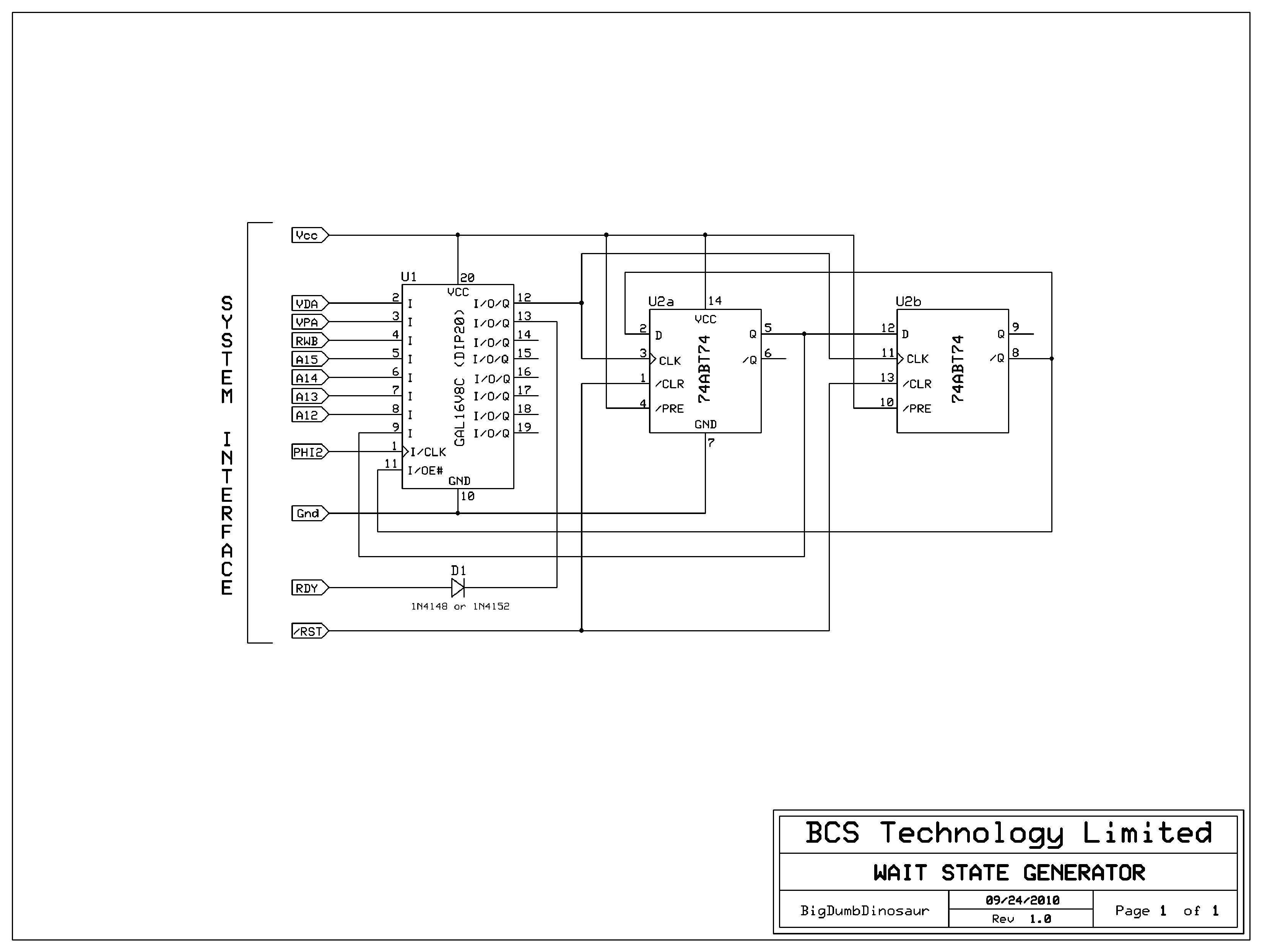
That's correct. The only fly in the ointment has to do with the NMOS 6502, which does not halt a write operation when RDY is asserted. That, of course, wouldn't be a problem with a ROM, but would definitely cause trouble writing to a slow peripheral device, e.g., the 2692 DUART in my POC design.

Quote:
My argument is, if you know the slower devices' access times, then why not have a changeable phase 2 with no wait states. One can change Phase 2 in the middle of software running without unintentionally crashing the CPU.

Why not? Because messing with Ø2 is more technically difficult than asserting and desasserting RDY. You have to be careful about when you slow down or speed up Ø2 so as to avoid MPU fatality. Sounds to me like a pointless kludge.

Quote:
...But I think it would maximize throughput because you are targeting access times.

I fail to see how monkeying with Ø2 is any more efficient than asserting RDY for one or two clock pulses. I could see slowing Ø2 on an NMOS MPU to deal with writes to slow hardware. With CMOS MPU's, there's no good reason to reduce the clock rate when RDY works as it should on write ops. How is reducing the clock rate going to "maximize throughput?"

_________________
x86?  We ain't got no x86.  We don't NEED no stinking x86!


Top
 Profile  
Reply with quote  
 Post subject:
PostPosted: Mon Nov 29, 2010 8:16 pm 
Offline
User avatar

Joined: Fri Aug 30, 2002 1:09 am
Posts: 8433
Location: Southern California
Quote:
How is reducing the clock rate going to "maximize throughput?"

Stretching φ2 by the minimum necessary amount for a given cycle, say 30%, is much better for throughput that adding a whole extra cycle, ie 100%. Circuitwise it would be pretty simple to do with an RC oscillator where you could have many different frequencies by switching parallel resistors in and out. I did a two-speed one in the 80's but it could have been many more, and there does not have to be any harmonic relation between the speeds.

It does of course mean a 6522's free-running T1 won't run and interrupt at the right speed. One possible solution is to use the PB6 input to run T2, so it would run at a consistent speed regardless, even if you upgrade things and make a big increase in clock speed which would otherwise require a software change to adjust for. It's not ideal though since T2 does not have the free-run feature with interrupt-on-rollover, and it also cannot automatically output a square wave on PB7.

If possible, I would rather just work on bringing up the speed of the slowest parts, so everything works near the processor's own speed limit. Wait states add to the variations in interrupt latency, increasing jitter when I don't want it.


Top
 Profile  
Reply with quote  
 Post subject:
PostPosted: Thu Dec 02, 2010 3:54 pm 
Offline
User avatar

Joined: Fri Aug 30, 2002 9:02 pm
Posts: 1685
Location: Sacramento, CA
BDD,

I have successfully incorporated the two Flip-flops (FF) into the 16V8 using the design you provided. While doing so, it occurred to me that you could do this with just one FF.

You let PHI2 drive the clock input. /RESET drives the /CLR input.

You place an AND gate on the D input with the /Q output of the FF going to one AND input and the Trigger (Address decoding) going to the other AND input.

Image

When the address is decoded as a slow device, the WS_EN input goes high. When PHI2 rises, Q goes high and /Q goes low, generating the RDY pulse. This also causes the AND gate output to go low, so the next PHI2 rising edge with set Q low and /Q high, removing the RDY.

I will update the 16V8 code to implement this setup and run the simulator.

I will post results back here when I'm done.

The use of the diode on the RDY pin is recommended to provide the isolation you described in your design. I'm not sure the tri-state output is needed unless you have more than one input to the RDY pin. However, this could be included in the new configuration as well.

Comments welcome.

Daryl


Top
 Profile  
Reply with quote  
 Post subject:
PostPosted: Thu Dec 02, 2010 6:53 pm 
Offline

Joined: Sat Jan 04, 2003 10:03 pm
Posts: 1706
While browsing idly the Internet last night (due primarily to my inability to sleep, in turn due to an upset stomach), I came across this document:

http://apple2online.com/web_documents/a ... _65-79.pdf

If you look on pages 9 through 15, you'll find some text that may be relevant to both the use of RDY and the use of clock-stretching (it appears the IIgs uses both techniques under a rather confusing set of different conditions).

I just thought I'd pass this on. It seemed interesting.


Top
 Profile  
Reply with quote  
PostPosted: Thu Dec 02, 2010 8:30 pm 
Offline
User avatar

Joined: Thu May 28, 2009 9:46 pm
Posts: 8178
Location: Midwestern USA
8BIT wrote:
I have successfully incorporated the two Flip-flops (FF) into the 16V8 using the design you provided. While doing so, it occurred to me that you could do this with just one FF.

I'm wondering if implementing this on a 20V8 or 22V10 might leave enough room for a second flop. That way the circuit could be jumper selectable for one or two wait-states. Or it might be possible to have the circuit automatically provide the right number of wait-states based upon the selected address. For example, ROM might be okay with one wait-state but two might be required with an I/O device.

In my POC V2 unit, which was designed around the wait-state circuit with the external flops, I arranged it so I could select one or two wait-states as I debugged the design. The goal is to run the thing at 20 MHz. Timing analysis suggests that I should be able to get away with one wait-state but I figured that having the ability to enable two would be a good idea, just in case my analysis is flawed.

I like your simplification and am eager to see how you fit it to a GAL.

BTW, I'm also evaluating the use of an Atmel ATF2500C PLD in my POC V2 design. Its greater capacity might allow me to combine the functions of the two GALs in the POC V2 into a one chip solution, including the flops. The 2500C is available in PDIP40 or PLCC44, the latter being stocked by Mouser and several others. Only things is my burner can't program the 2500C, so I may have to go shopping for a new one. :(

_________________
x86?  We ain't got no x86.  We don't NEED no stinking x86!


Top
 Profile  
Reply with quote  
 Post subject:
PostPosted: Thu Dec 02, 2010 8:52 pm 
Offline
User avatar

Joined: Thu May 28, 2009 9:46 pm
Posts: 8178
Location: Midwestern USA
kc5tja wrote:
While browsing idly the Internet last night (due primarily to my inability to sleep, in turn due to an upset stomach), I came across this document:

http://apple2online.com/web_documents/a ... _65-79.pdf

If you look on pages 9 through 15, you'll find some text that may be relevant to both the use of RDY and the use of clock-stretching (it appears the IIgs uses both techniques under a rather confusing set of different conditions).

I just thought I'd pass this on. It seemed interesting.

It is and illustrates some of the complexities of trying to be all things to all men.

The IIgs was designed so expansion hardware made for the older IIe could be used. Unfortunately (for Apple), this gave rise to clock complications (not unlike what Commodore had to grapple with in the C-128) and these, in turn, complicated wait-stating. While the 65C816 uses a single clock (PHI2) for all timing, the IIe's 65C02 did not, and therefore, Apple had to synthesize a PHI0 and PHI1 clock to satisfy the timing requirements of the older hardware. I can only imagine what expansion card designers targeting the IIga must've thought the first time they had to figure it which clock to use and when specific hardware conditions would be valid.

In the tech docs, an interesting comment is made that supports a long-time assertion of mine about when to assert RDY on the '816: do not assert it when PHI2 is low, as it will result in an invalid bank address being latched. Apple apparently had to kludge the design a bit to deal with this problem (see page 11 in the above reference document).

_________________
x86?  We ain't got no x86.  We don't NEED no stinking x86!


Top
 Profile  
Reply with quote  
PostPosted: Thu Dec 02, 2010 8:59 pm 
Offline

Joined: Thu Sep 02, 2010 12:34 am
Posts: 36
Location: Salzburg, Austria
Hi!
BigDumbDinosaur wrote:
BTW, I'm also evaluating the use of an Atmel ATF2500C PLD in my POC V2 design. Its greater capacity might allow me to combine the functions of the two GALs in the POC V2 into a one chip solution, including the flops. The 2500C is available in PDIP40 or PLCC44, the latter being stocked by Mouser and several others. Only things is my burner can't program the 2500C, so I may have to go shopping for a new one. :(

Wouldn't it be easier to use a XC9536XL or XC9572XL? They are available in PLCC44, too, can be programmed with a simple JTAG cable and seem to be a lot cheaper (Digikey lists the XC9536XL for ~1USD, the ATF2500C costs ~6-8 USD).

so long,

Hias


Top
 Profile  
Reply with quote  
PostPosted: Thu Dec 02, 2010 9:38 pm 
Offline
User avatar

Joined: Thu May 28, 2009 9:46 pm
Posts: 8178
Location: Midwestern USA
HiassofT wrote:
Wouldn't it be easier to use a XC9536XL or XC9572XL? They are available in PLCC44, too, can be programmed with a simple JTAG cable and seem to be a lot cheaper (Digikey lists the XC9536XL for ~1USD, the ATF2500C costs ~6-8 USD).

Probably no easier in terms of expressing the logic. The cost of the part itself isn't particularly important at this stage, as I don't have any immediate plans to mass-produce this thing. :)

More significantly, the XL9536 and XL9572 are 3.3 volt parts, which would preclude their use to control standard 5 volt CMOS parts. I don't want to have to consume PCB real estate with voltage level converters (and the propagation delay they produce).

_________________
x86?  We ain't got no x86.  We don't NEED no stinking x86!


Top
 Profile  
Reply with quote  
PostPosted: Thu Dec 02, 2010 10:12 pm 
Offline

Joined: Thu Sep 02, 2010 12:34 am
Posts: 36
Location: Salzburg, Austria
BigDumbDinosaur wrote:
Probably no easier in terms of expressing the logic. The cost of the part itself isn't particularly important at this stage, as I don't have any immediate plans to mass-produce this thing. :)

OK, good points.

Quote:
More significantly, the XL9536 and XL9572 are 3.3 volt parts, which would preclude their use to control standard 5 volt CMOS parts. I don't want to have to consume PCB real estate with voltage level converters (and the propagation delay they produce).

This, however, is not an issue. Although the XC95..XL series are running at 3.3V, the I/Os are guaranteed to be 5V tolerant. So all you need is a small 3.3V voltage regulator sitting somewhere.

So far I successfully used the XC9536XL in one project (a RAM upgrade for the Atari 800XL) and currently I'm working on another project using the XC95144XL (in TQ100). A prototype is sitting on my desk, first few experiments worked fine. I'm just glad I didn't have to solder this by myself (a friend did the PCBs and the soldering), TQ100 is - erm - quite fine-pitch :-)

so long,

Hias


Top
 Profile  
Reply with quote  
 Post subject:
PostPosted: Thu Dec 02, 2010 10:27 pm 
Offline

Joined: Tue Jul 05, 2005 7:08 pm
Posts: 993
Location: near Heidelberg, Germany
8BIT wrote:
When the address is decoded as a slow device, the WS_EN input goes high. When PHI2 rises, Q goes high and /Q goes low, generating the RDY pulse. This also causes the AND gate output to go low, so the next PHI2 rising edge with set Q low and /Q high, removing the RDY.


That requires that the address decoding to detect a slow device is done before phi2 rises. That can create some timing constraints for higher clock speeds.

But actually I've used a phi2-rising-edge-based design myself, but only at max 2MHz http://www.6502.org/users/andre/icaphw/rdy.html. Oops, looking at the schematics again, I am actually using phi2 rising edge in my CS/A 65816 board as well, which runs at 8MHz :-)

So this would still work for some higher speeds, yet I'd look carefully at the timing.

Also your design automatically restricts RDY to a single cycle - which is often enough, though.

André


Top
 Profile  
Reply with quote  
Display posts from previous:  Sort by  
Post new topic Reply to topic  [ 51 posts ]  Go to page 1, 2, 3, 4  Next

All times are UTC


Who is online

Users browsing this forum: No registered users and 5 guests


You cannot post new topics in this forum
You cannot reply to topics in this forum
You cannot edit your posts in this forum
You cannot delete your posts in this forum
You cannot post attachments in this forum

Search for:
Jump to: