6502.org Forum  Projects  Code  Documents  Tools  Forum
It is currently Fri Sep 20, 2024 4:08 am

All times are UTC


Post new topic Reply to topic  [ 56 posts ]  Go to page Previous  1, 2, 3, 4  Next
Author Message
PostPosted: Mon Apr 16, 2012 5:32 am 
Offline
User avatar

Joined: Tue Nov 16, 2010 8:00 am
Posts: 2353
Location: Gouda, The Netherlands
ElEctric_EyE wrote:
Ok, so your CPU is running at 100MHz as is your SDRAM video controller. I assume the CPU is your original 8 bit version?

Yes, everything is running at 100 MHz. I've never tried running things at different clock frequencies, and honestly I have no idea how to do it, except in the "easy" cases where the clock domains can be separated by a dual port RAM. The core is a slightly modified version of the 8 bit original. I have removed a few cycles at the cost of an extra adder in the address calculator. Also, I moved the stack page into page zero. I didn't need so much zero page/stack, so now I have extra room for code.
Quote:
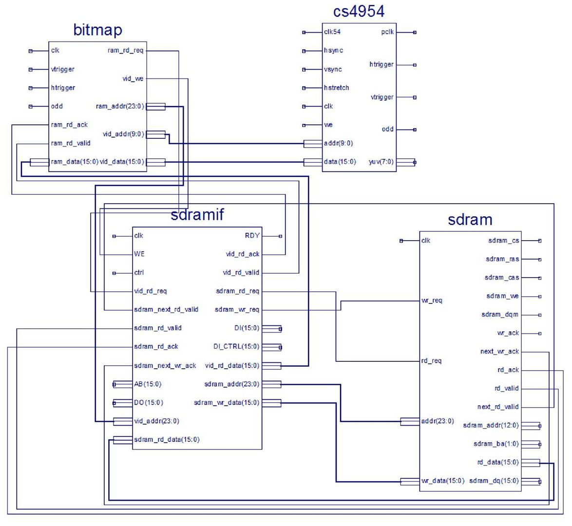
I would like to experiment with your SDRAM code

Attached. Note that the sdramif.v module is made for an 8 bit CPU. For the 65org16 core you'll need to modify a few things.
Code:
        sdram_wr_data <= { DOH, DO };
        sdram_addr <= { ABH, AB[7:0] };

Should be changed into:
Code:
        sdram_wr_data <= DO;
        sdram_addr <= AB[23:0];

And some of the signals need to be changed from 8 to 16 bit.
You can also remove this code here:
Code:
always @(posedge clk)
    if( ctrl & WE )
        case( AB[1:0] )
            0: ABH[ 7:0] <= DO;
            1: ABH[15:8] <= DO;
            2: DOH       <= DO;
        endcase


By the way, I'm not too happy with the design of the sdramif module. It's a bit of a quick hack. It seems to work okay, but I would like to replace it with a cleaner design at some point.


Attachments:
File comment: Verilog sources for SDRAM controller
65org16dev.zip [13.92 KiB]
Downloaded 109 times
Top
 Profile  
Reply with quote  
PostPosted: Mon Apr 16, 2012 11:45 am 
Offline

Joined: Mon Mar 02, 2009 7:27 pm
Posts: 3258
Location: NC, USA
I'll have to use an older 100MHz version of .b core. Thanks so much for your contributions, it is much appreciated! I have some little troubleshooting left on my board, then I can dive in. I've put much time recently into understanding and expanding your original 6502 core, but I think I need a rest from that now.

_________________
65Org16:https://github.com/ElEctric-EyE/verilog-6502


Top
 Profile  
Reply with quote  
PostPosted: Mon Apr 16, 2012 12:04 pm 
Offline
User avatar

Joined: Tue Nov 16, 2010 8:00 am
Posts: 2353
Location: Gouda, The Netherlands
ElEctric_EyE wrote:
I'll have to use an older 100MHz version of .b core.

Not necessarily. The code I have attached will work fine at 90 MHz or even lower. The only issues I can think of are: the generation of the 24MHz and 54 MHz clocks for USB and video, which are both derived from the 100 MHz oscillator, and also the SDRAM refresh time.

The SDRAM refresh can be modified in the sdram.v file. Replace the number 768 with a smaller number to get more frequent refresh cycles.
Code:
        refresh_count <= refresh_count - 16'd768;


ETA: with 768 you get a nominal refresh cycle every 768 / 100 = 7.68 usecs. The SDRAM requires 8192 refresh cycles every 64 ms. I have a mechanism in the SDRAM controller where it can delay up to 32 refresh cycles when it's busy. So, worst case I get 8192 refresh cycles in (8192+32)*7.68 = 63.2 ms.


Top
 Profile  
Reply with quote  
PostPosted: Mon Apr 16, 2012 9:00 pm 
Offline

Joined: Mon Mar 02, 2009 7:27 pm
Posts: 3258
Location: NC, USA
Arlet wrote:
... Also, I moved the stack page into page zero. I didn't need so much zero page/stack, so now I have extra room for code.

This is true of the 65Org16.x too!
This is definately a wise decision IMO. I will modify my testbech and cpu and see if there is any speed increase!

_________________
65Org16:https://github.com/ElEctric-EyE/verilog-6502


Top
 Profile  
Reply with quote  
PostPosted: Thu Jun 07, 2012 7:40 pm 
Offline

Joined: Mon Mar 02, 2009 7:27 pm
Posts: 3258
Location: NC, USA
Just to finish up my last comment, I didn't notice any speed increase when I put the stack and zero page in the same 64K block with the stack on top. 1Kx16 each...

For bitmap generation only, no sprites, using the SDRAM, can I use 4 modules as connected here?

Sorry, this is a poor quality picture. I'll make a larger one tonight.

EDIT: Added a larger pic just now, will take some time to update.

_________________
65Org16:https://github.com/ElEctric-EyE/verilog-6502


Top
 Profile  
Reply with quote  
PostPosted: Fri Jun 08, 2012 5:19 am 
Offline
User avatar

Joined: Tue Nov 16, 2010 8:00 am
Posts: 2353
Location: Gouda, The Netherlands
ElEctric_EyE wrote:
EDIT: Added a larger pic just now, will take some time to update.

It's still small, but there are some loose signals on the bitmap module (trigger/odd) that need to be connected to the cs4954 module.


Top
 Profile  
Reply with quote  
PostPosted: Fri Jun 08, 2012 12:33 pm 
Offline

Joined: Mon Mar 02, 2009 7:27 pm
Posts: 3258
Location: NC, USA
Ok, the size issue should be fixed now.

I see I missed those 3 signals. I have more than a few questions on how to properly hook this up, so please bear with me.

1) Is the vid_we signal from the bitmap module routed correctly?
2) The pixel clock (pclk) from the CS4954 module goes to the bitmap module. The system/cpu clock goes to the clk inputs of the CS4954, SDRAM, and SDRAMIF modules?

_________________
65Org16:https://github.com/ElEctric-EyE/verilog-6502


Top
 Profile  
Reply with quote  
PostPosted: Fri Jun 08, 2012 1:00 pm 
Offline
User avatar

Joined: Tue Nov 16, 2010 8:00 am
Posts: 2353
Location: Gouda, The Netherlands
ElEctric_EyE wrote:
Ok, the size issue should be fixed now.

1) Is the vid_we signal from the bitmap module routed correctly?
2) The pixel clock (pclk) from the CS4954 module goes to the bitmap module. The system/cpu clock goes to the clk inputs of the CS4954, SDRAM, and SDRAMIF modules?


The vid_we signal should go to the CS4954 module. It controls the vid_addr/vid_data bus.

The bitmap module runs on the system/cpu clock. The same clock goes to the clk input of the CS4954. A 54 MHz clock goes into the clk54 input, and a 27 MHz clock comes out of the pclk signal, which needs to go to the video clock output of the FPGA to the CS4954 chip.


Top
 Profile  
Reply with quote  
PostPosted: Fri Jun 08, 2012 2:05 pm 
Offline

Joined: Mon Mar 02, 2009 7:27 pm
Posts: 3258
Location: NC, USA
Excellent, thanks!

3) In the code for sdramif.v, there's a comment for the 'ctrl' input saying it's used for window control. It's related to the DI_CTRL[15:0]? How does this output work?

EDIT: N/M, I see 'ctrl' is related to the section you said to comment out for interfacing to an 16-bit cpu. So I don't need to use the DI_CTRL output? What is AB[15:0] used for?

_________________
65Org16:https://github.com/ElEctric-EyE/verilog-6502


Top
 Profile  
Reply with quote  
PostPosted: Fri Jun 08, 2012 3:43 pm 
Offline
User avatar

Joined: Tue Nov 16, 2010 8:00 am
Posts: 2353
Location: Gouda, The Netherlands
ElEctric_EyE wrote:
3) In the code for sdramif.v, there's a comment for the 'ctrl' input saying it's used for window control. It's related to the DI_CTRL[15:0]? How does this output work?

EDIT: N/M, I see 'ctrl' is related to the section you said to comment out for interfacing to an 16-bit cpu. So I don't need to use the DI_CTRL output? What is AB[15:0] used for?


An 8 bit CPU, like the 6502, would first perform two byte writes to special control registers. These would be stored in ABH[15:8] and ABH[7:0], and set the SDRAM page. Then the CPU could do a bunch of accesses to page $A0xx, where the lower 8 bits of the address would be concatenated as follows:
Code:
        sdram_addr <= { ABH, AB[7:0] };

With a 32 bit address bus, you could map the SDRAM to $A0xxxxxx instead. Remove ABH, and use:
Code:
        sdram_addr <= AB[23:0] ;


Top
 Profile  
Reply with quote  
PostPosted: Fri Jun 08, 2012 5:16 pm 
Offline

Joined: Mon Mar 02, 2009 7:27 pm
Posts: 3258
Location: NC, USA
I have enough information to hook it all up now, thanks again for the help.

My project is reaching proportions now, that I can see I am going to have trouble fitting this video portion into my project in schematic form. My next challenge will have to be to learn how to create a top level in Verilog, instead of schematic before I can see any graphics. I can get some clues from ISE's HDL translation of my schematic, and also your main.v file.

_________________
65Org16:https://github.com/ElEctric-EyE/verilog-6502


Top
 Profile  
Reply with quote  
PostPosted: Wed Jun 20, 2012 11:05 am 
Offline

Joined: Mon Mar 02, 2009 7:27 pm
Posts: 3258
Location: NC, USA
Sorry, so many things going on in the summer months, with kids off from school I must keep them entertained for part of the day on my days off... Today I should be able to complete adding the 65Org16.b core, ZPRAM, STackRAM and a simple OSROM to your modules and hopefully see some video output. I've abandoned trying to merge my TFT project for now, with it's top level schematic. I think what will happen is I will slowly add parts of it in verilog to this new project...

Could you perchance post me your register settings for the CS4954 to save me some time?

_________________
65Org16:https://github.com/ElEctric-EyE/verilog-6502


Top
 Profile  
Reply with quote  
PostPosted: Wed Jun 20, 2012 11:21 am 
Offline
User avatar

Joined: Tue Nov 16, 2010 8:00 am
Posts: 2353
Location: Gouda, The Netherlands
Here's my NTSC init:
Code:
reg $00 = $12
reg $01 = $12
reg $03 = $01
reg $04 = $07
reg $05 = $78
reg $10 = $1C
reg $11 = $3E
reg $12 = $F8
reg $13 = $E0
reg $14 = $43


Top
 Profile  
Reply with quote  
PostPosted: Wed Jun 20, 2012 12:56 pm 
Offline

Joined: Mon Mar 02, 2009 7:27 pm
Posts: 3258
Location: NC, USA
Thanks for the quick response!
Just got done soldering in the SDRAM and .1uF bypass caps. Old TFT project, which was still loaded in FPGA FLASH, still boots up the TFT and color bars for S-Video meaning no power distribution/noise errors on this board. All other signals from FPGA to SDRAM are unused and therefore hi-impedance, except for the SDRAM /CS which I was forcing high. Taking baby steps here...

_________________
65Org16:https://github.com/ElEctric-EyE/verilog-6502


Top
 Profile  
Reply with quote  
PostPosted: Wed Jun 20, 2012 6:01 pm 
Offline

Joined: Mon Mar 02, 2009 7:27 pm
Posts: 3258
Location: NC, USA
I see your values are identical to the ones I used for the color bar test pattern. But, I thought the resolution had to be specified in order to set the appropriate HSYNC and VSYNC frequencies?

My design has passed synthesis, except for the timing constraint for the CPU. Looks close though... Running smartXplorer made it pass the 10ns constraint!

I guess this is a good initial observation that with this new design with your modules, the CS4954 is outputting color bar test pattern. So at least I know the address decoding is good, the CPU is running fine with your I2C routine, and the StackRAM and ZeroPageRAM are functioning.

_________________
65Org16:https://github.com/ElEctric-EyE/verilog-6502


Top
 Profile  
Reply with quote  
Display posts from previous:  Sort by  
Post new topic Reply to topic  [ 56 posts ]  Go to page Previous  1, 2, 3, 4  Next

All times are UTC


Who is online

Users browsing this forum: No registered users and 8 guests


You cannot post new topics in this forum
You cannot reply to topics in this forum
You cannot edit your posts in this forum
You cannot delete your posts in this forum
You cannot post attachments in this forum

Search for:
Jump to: