
First attempt with new SDRAM controller design appears to be working. I first noticed some read/write errors, but that seems to be fixed by slightly changing the SDRAM clock phase relationship. Edit: There's a still a bit of work to do. Parts of the state machine are still empty, but the access patterns of the 6502 don't lead it into those states.
I'm not actually sure what the timing should be to capture the data right in the middle of the eye, so I'm just moving the clock around until it works. My 200 MHz scope isn't fast enough, and whatever I see doesn't seem to match simulation.
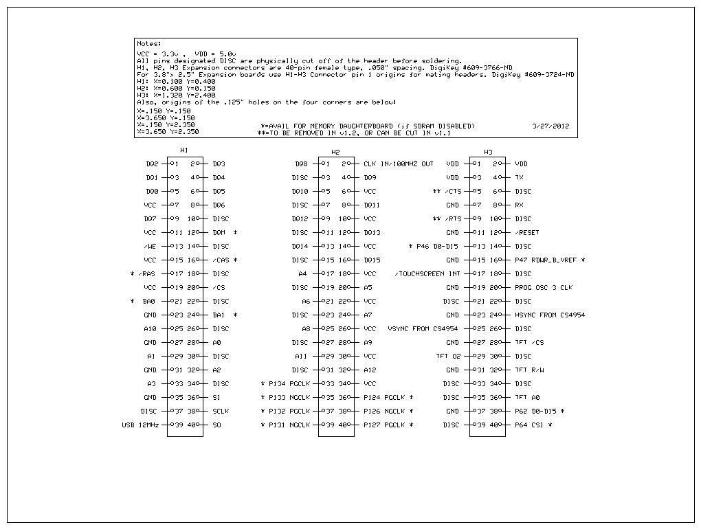
65Org16.x Dev. Board V1.1 using a Spartan 6 XC6SLX9-3TQG144
Last edited by Arlet on Tue Mar 27, 2012 6:32 pm, edited 1 time in total.
ElEctric_EyE wrote:
Yes, the SPI pins are on Header #1, but the physical SD card connector would have to go on the daughterboard without modifying the current mainboard. So the SPI interface would have to go onto a CPLD at least I would think...
-
ElEctric_EyE
- Posts: 3260
- Joined: 02 Mar 2009
- Location: OH, USA
I updated the 1st post to include the correct Header pinout. The pic should update soon...
It shows 18 pins available for a SyncRAM daughterboard. 9 pins for A13-A21 (for the largest device), 8 CSs, and 1 /CS for the SD Card...
Take 5 of those away for the SDRAM signals on a SDRAM daughterboard. That leaves 13, for 12 SDRAM CSs and the 1 /CS for the SD Card.
No need for another CPLD/FPGA for a controller core!
Last edited by ElEctric_EyE on Tue Mar 27, 2012 9:35 pm, edited 1 time in total.
-
ElEctric_EyE
- Posts: 3260
- Joined: 02 Mar 2009
- Location: OH, USA
-
ElEctric_EyE
- Posts: 3260
- Joined: 02 Mar 2009
- Location: OH, USA
Side note: I am seeing the data shifted out on SDA, the SCL just goes low during the shift... Not only did I find that my core was not doing load_reg for <shift,rotate> opcodes in the 6 & E columns (which I fixed), your routine is doing an ROL (op $26) meant for an 8 bit machine! So my carry flag isn't being set in time (I think).
ElEctric_EyE wrote:
Side note: I am seeing the data shifted out on SDA, the SCL just goes low during the shift... Not only did I find that my core was not doing load_reg for <shift,rotate> opcodes in the 6 & E columns (which I fixed), your routine is doing an ROL (op $26) meant for an 8 bit machine! So my carry flag isn't being set in time (I think).
You can fix the ROL by moving the data 8 bits to the left before you enter the loop.

BigEd wrote:
Arlet:
nice idea for the tiny code buffer - a bit like a 68010 perhaps. You'll need to make some statement about self-modifying code (as with all instruction caching)
nice idea for the tiny code buffer - a bit like a 68010 perhaps. You'll need to make some statement about self-modifying code (as with all instruction caching)
Partially working attempt to use new SDRAM controller in combination with video interface. I made a simple module to read a bitmap from the SDRAM, and send it to the display. It's currently showing the random initial contents of the SDRAM.
When I try to combine the video read with CPU access to the SDRAM, the screen turns black. Apparently, some state machine gets stuck.
When I try to combine the video read with CPU access to the SDRAM, the screen turns black. Apparently, some state machine gets stuck.
6502.org wrote:
Image no longer available: http://ladybug.xs4all.nl/arlet/fpga/sdram.jpg
-
ElEctric_EyE
- Posts: 3260
- Joined: 02 Mar 2009
- Location: OH, USA
Graphics! Awesome!!
Side note:
Yes I got it backwards, SCL was toggling SDA was going low. I've shifted the 'addr' and 'val' values 8bits to the left immediately before the 'jsr i2c_wrbyte' in all 3 instances in the 'video_write_reg' routine.
I'm close now, but just 1 question: We are sending 3 bytes. First the device I2C address, then the internal register address, then the value? I must take into consideration I may have rewrote the default address of the CS4954...
Side note:
Arlet wrote:
Hmm... don't you mean that the SCL is toggling, but the SDA just goes low ? That would match the behavior of the ROL on a 16 bit target. The SCL is just pulled up and down by calls to scl_low and scl_high.
You can fix the ROL by moving the data 8 bits to the left before you enter the loop.
You can fix the ROL by moving the data 8 bits to the left before you enter the loop.
I'm close now, but just 1 question: We are sending 3 bytes. First the device I2C address, then the internal register address, then the value? I must take into consideration I may have rewrote the default address of the CS4954...
ElEctric_EyE wrote:
I'm close now, but just 1 question: We are sending 3 bytes. First the device I2C address, then the internal register address, then the value?
Quote:
I must take into consideration I may have rewrote the default address of the CS4954...
Fixed the SDRAM state machine, so now the 6502 core can write to SDRAM while video is reading it. It's not perfect yet, because some pixels are not written in the right color, resulting in some random speckle pattern instead of a solid black bar. Edit: Ah, good! The speckle pattern also shows up in simulation, so it's a logic error, and not some tricky analog/timing problem.
Too bad the 6502 address space is only 16 bit At 720*480 resolution and 16 bits per pixel, the core can only access a small section. Of course, the 65org16 has no problem accessing the amount of memory. However, it may become a bit sluggish when scrolling the screen in software.
Too bad the 6502 address space is only 16 bit
-
ElEctric_EyE
- Posts: 3260
- Joined: 02 Mar 2009
- Location: OH, USA
Arlet wrote:
...Too bad the 6502 address space is only 16 bit At 720*480 resolution and 16 bits per pixel, the core can only access a small section. Of course, the 65org16 has no problem accessing the amount of memory. However, it may become a bit sluggish when scrolling the screen in software.
That is before all the tinkering started with modifying your core...
ElEctric_EyE wrote:
Now see, this is why I got all excited when BigEd originally said he had expanded your core to a 16bit databus. Writing graphics routines for anything over 256x256 resolution was a pain for me with the original 8bit 6502, but I did it... Working with a 320x200 TFT at the time, I was forced to do it. That is before all the tinkering started...
But I want to use the FPGA to write to the screen instead of the CPU. That's why I made the text rendering module, where the entire screen can be accessed quickly by writing only a 2kB memory region. Now, instead of rendering real-time to the display, the hardware could be modified to write the image to a section of SDRAM. That piece of SDRAM could then be displayed on the screen, or modified further. Ideally, the hardware would do nearly all of the graphics manipulation and the CPU would just direct traffic.