6502.org
http://forum.6502.org/

Working with Xilinx BGA packages
http://forum.6502.org/viewtopic.php?f=10&t=2070
Page 2 of 10

Author:  ElEctric_EyE [ Thu Mar 28, 2013 2:27 pm ]
Post subject:  Re: Working with Xilinx BGA packages

The timing of your post is amazing. I have to seriously start considering purchasing the tools very soon. My project cannot fit the pseudo random number generator and the timer with everything else and maintain 100MHz with the 144-pin Spartan 6. Up to 14 modules now, and I still have more to do with the video mixing.
With a package using more pins I could do what I wanted to do and utilize the 2 parity bits on the address lines of the SyncRAM and assign 4 math/logic functions to every pixel.
I will start searching out a good size Spartan 6. Thanks for the inspiration!

EDIT: Added detail. Was busy day at work when I had posted earlier.

Author:  enso [ Sun Jun 02, 2013 4:39 am ]
Post subject:  Re: Working with Xilinx BGA packages

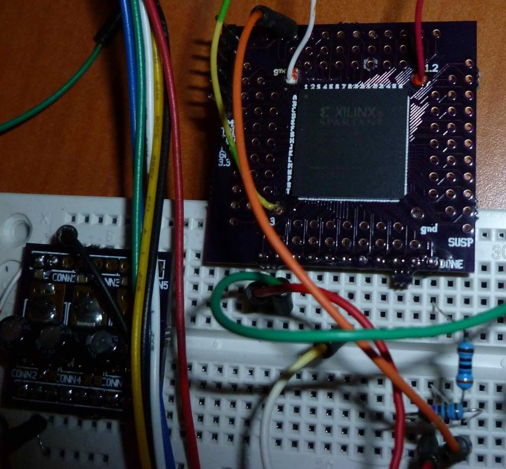
XC3S200AN 256-pin BGA successfully mounted. It configures, and I've tested a bunch of the connected pins with an LED blinker circuit...
Soldered using a hunk-of-aluminum PID hotplate, homemade.

I am sick of the flaky breadboards, though. Anyone else interested in a wire-wrap breakout board for BGA chips?

Image

Author:  enso [ Mon Jun 10, 2013 6:51 pm ]
Post subject:  Re: Working with Xilinx BGA packages

I would like to report another mounting success, this time with a 484 BGA package:
Image
Here is an edge view, showing how you can see underneath the chip. This gives you a pretty good indication that there are no shorts - you can see down the entire grid!
Attachment:
P1000827.resized.JPG
P1000827.resized.JPG [ 166.63 KiB | Viewed 1700 times ]

I soldered down 3 of these BGAs perfectly.

Unfortunately my PCB had an error with power distribution, so the board is running hot because the VCCINT bus is being fed 3.3V. Amazingly it works (who knows for how long though) - see http://forum.6502.org/viewtopic.php?f=10&t=2328&start=15

Author:  ElEctric_EyE [ Mon Jun 10, 2013 10:30 pm ]
Post subject:  Re: Working with Xilinx BGA packages

Very good news! Nice to hear you figured out your issue with VCCint and VCCaux... So you have a 2 layer board and a 484-pin device. How many of the pins are unused? I am itching to start a new design and tackle a larger Spartan 6. Thanks for posting.

Author:  enso [ Mon Jun 10, 2013 10:57 pm ]
Post subject:  Re: Working with Xilinx BGA packages

BGA484 is greatly underutilized in my case, but it was more than enough IOs for my purposes.

With a two-layer board, in the ideal case you can bring out 4 rows (2 on top layer and 2 on the bottom layer), from each of the 4 sides. In practice (once you try you'll see why) the yield is lower. But with 22 rows of pins, even 2 layers gives you 22 x 4 = 88 pins, and you can easily take out more than 100.

If you need a lot more, I would just use the BGA 1154 package, with rows of 34 pins. You can easily take 400 pins out of that one, and the wider chip gives you more room to route around - not to mention that there are more goodies inside!

My thinking is to not worry too much about the 'wasted' pins, and just enjoy myself...

I do want to point out that if you plan to make a fast core using Spartan6, consider that not having a groundplane may be problematic...

Here is the relevant piece of the PCB: (Click to enlarge. .) Note there are a few IO lines that I just didn't have room to route anywhere, so I attached them to long narrow pads that can be used to attach wire-wrap wire for future expansion.

Attachments:
b.png
b.png [ 121.38 KiB | Viewed 1716 times ]

Author:  ElEctric_EyE [ Tue Jun 11, 2013 1:07 am ]
Post subject:  Re: Working with Xilinx BGA packages

How much cost and what parts were involved in your PID hotplate custom construction? I think you laid out a few parts for your thread in the hardware section? or somewhere, but not really any of the full details. If I missed the thread just point there. I remember an aluminum block with 2 connections.

Author:  enso [ Tue Jun 11, 2013 1:37 am ]
Post subject:  Re: Working with Xilinx BGA packages

Parts for the hotplate:
    aluminum block. Size not too important; mine is about 1" x 4" x 7"
    pid controller
    ssr - solid state relay
    thermocouple
    heating elements - I used 2 x 500W units (it takes about 10min to heat up to 250C)

You can get these on amazon, ebay or anywhere in China. Total cost should be <$75, especially if you can get the aluminum block locally.

Make sure the PID controller can use a thermocouple - I think all of them can.

Heaters and thermocouples come in all sizes - pick one that will fit inside your aluminum block.

Once you have them, drill your block. Don't even think about using a hand drill, use a good, long-travel drill press or you'll be sorry. I was sorry - my drill press could not travel far enough, and my drill bit was too short. Needless to say, using the wrong tools just makes your job harder - each hole required readjustments of the drill press mid-drilling.

Then insert heating elements and the 'couple. Mine was big enough for 2 heaters - a single one for a smaller block is probably fine. The thermocouple hole was threaded, the heaters just pressure-fit into holes.

The rest is making electrical connections and deciphering the PID instructions. I used the default PID tuning settings - it's good enough. Pulses the heaters about once per second.
Attachment:
P1000828.resized.JPG
P1000828.resized.JPG [ 185.09 KiB | Viewed 1701 times ]

Attachment:
P1000829.resized.JPG
P1000829.resized.JPG [ 201.3 KiB | Viewed 1701 times ]


I am not sure if the hotplate is really better than an oven. For experimenting, definitely - you can see your board better. But an oven is better for attaching lots of chips on both sides of the board.

Author:  enso [ Tue Jun 11, 2013 4:15 am ]
Post subject:  Re: Working with Xilinx BGA packages

Some thoughts on mounting BGAs at home

After much trial and error, I would like to tell you this:

BGAs are well within the realm of an advanced hobbyist! In fact, BGAs are easier than TQFPs

    1mm is easier to place than 0.5mm.

    Don't use solderpaste (m̶y̶ ̶P̶C̶B̶ ̶v̶e̶n̶d̶o̶r̶ ̶g̶o̶l̶d̶-̶p̶l̶a̶t̶e̶s̶ ̶t̶h̶e̶ ̶b̶o̶a̶r̶d̶s̶,̶ ̶o̶t̶h̶e̶r̶ ̶f̶i̶n̶i̶s̶h̶e̶s̶ ̶m̶a̶y̶ ̶r̶e̶q̶u̶i̶r̶e̶ ̶p̶a̶s̶t̶e̶). [2021 edit: No gold-plated boards! Use regular tinned boards and no paste! ] Just liquid flux from a pen. Balls melt enough to provide a solid connection. Without paste, you can move the chip around until it pops into the dips made by the soldermask, so placing is easy! You hardly need a magnifier.

    Hotplate makes the process easy as you can see the balls soften and the chip slump. You can then gently remove your board and cool it. I ruined a number of BGAs in the oven by over and undercooking. My oven is not PID controlled. If you are more scientific about it, you will be able to do it, but with a plate you can just watch the balls.

    Prepare to ruin a few chips before getting the hang of it. I ruined a few because of solderpaste, which is a bad idea. As it melts, it transfers too much heat to the balls, and the whole chip just crashes down squeezing molten solder out the side.

    You don't need an X-ray machine! You can look at your BGA from the side, right through every row of balls to verify that there are no shorts. And the balls themselves around the edges give you a very good idea of how well the part is attached. If it's symmetrical and the edge balls are well-formed, and you can see through it, you are done. I haven't had a single problem yet.

    The hard part is not the soldering, it's laying out an error-free circuit connecting all those pads under the chip. Breaking out from the grid is a real puzzle - you can't put vias under pins (they suck solder right out); there is only one place to put a via - smack in between 4 pads. Once you put a via, you can't put a wire there, so it's a lot like a Rubik's cube.

    All PCB layout packages simply stink when it comes to dense BGA grids. I use gEDA PCB - it's quirky but at least it's opensource and the files are text-based, so I can generate tricky footprints or adjust placement of things with a text editor on occasion.

Author:  GARTHWILSON [ Tue Jun 11, 2013 5:21 am ]
Post subject:  Re: Working with Xilinx BGA packages

enso wrote:
you can move the chip around until it pops into the dips made by the soldermask, so placing is easy! You hardly need a magnifier.

What kind of soldermask? Would this work with LPI, or only with wet-screened? (Is LPI thick enough to do this?)

Quote:
My oven is not PID controlled. If you are more scientific about it, you will be able to do it, but with a plate you can just watch the balls.

Would an electric skillet work?

Quote:
The hard part is not the soldering, it's laying out an error-free circuit connecting all those pads under the chip. Breaking out from the grid is a real puzzle - you can't put vias under pins (they suck solder right out)

What if you fill the via with solder first? It kind of sounds like the BGA manufacturers almost assume you're going to make a multilayer board with blind and burried vias. That's not cheap stuff.

Quote:
All PCB layout packages simply stink when it comes to dense BGA grids. I use gEDA PCB - it's quirky but at least it's opensource and the files are text-based, so I can generate tricky footprints or adjust placement of things with a text editor on occasion.

I use an old DOS version of Easy-PC Pro. It was only $375 nearly 20 years ago, but I like it because it is so flexible it lets me do almost anything I want, including a lot of things the programmers probably didn't think of. (The advent of Gerber 274X helped with this, because it used to be a pain to explain the merge files to the board houses when all we had was 274D and had to write things up in clear detail in the manufacturing instructions.) I always make my own custom land patterns because I can get better density that way than what comes standard, and we have not had any resulting production problems. I have the book "SMT High Density Design & DFM" by James C. Blankenhorn, put out by SMT Plus, Inc.. It cost something like $300 but it is poorly written and their idea of high density is not very dense compared to what we've been doing. It does not have anything about BGAs though; so what would you recommend for the sizes and shapes of the land pattern pads? It looks like you used round ones. Should I assume that the BGA manufacturers have pad-size recommendations like manufacturers have for other packages? Should the holes in the soldermask be only big enough to ensure that there's no gasketing (which would mean only about .002" or .004" greater diameter than the pad if it's LPI)?

Author:  Arlet [ Tue Jun 11, 2013 5:32 am ]
Post subject:  Re: Working with Xilinx BGA packages

GARTHWILSON wrote:
Should I assume that the BGA manufacturers have pad-size recommendations like manufacturers have for other packages? Should the holes in the soldermask be only big enough to ensure that there's no gasketing (which would mean only about .002" or .004" greater diameter than the pad if it's LPI)?

Yes, the BGA manufacturers generally have good recommendations with respect to pads, soldermask, clearance, traces and vias. See for instance Xilinx Device Package User Guide.

Author:  Arlet [ Tue Jun 11, 2013 5:38 am ]
Post subject:  Re: Working with Xilinx BGA packages

enso wrote:
Don't use solderpaste (my PCB vendor gold-plates the boards, other finishes may require paste). Just liquid flux from a pen. Balls melt enough to provide a solid connection. Without paste, you can move the chip around until it pops into the dips made by the soldermask, so placing is easy! You hardly need a magnifier.

A friendly manufacturer recommended that I should use solderpaste for BGA. I did, and it worked, but it definitely requires very careful work, especially when placing the component.

Author:  GARTHWILSON [ Tue Jun 11, 2013 6:34 am ]
Post subject:  Re: Working with Xilinx BGA packages

Arlet wrote:
Yes, the BGA manufacturers generally have good recommendations with respect to pads, soldermask, clearance, traces and vias. See for instance Xilinx Device Package User Guide.

Thanks. Very complete.

Author:  enso [ Tue Jun 11, 2013 6:50 am ]
Post subject:  Re: Working with Xilinx BGA packages

GARTHWILSON wrote:
What kind of soldermask? Would this work with LPI, or only with wet-screened? (Is LPI thick enough to do this?)

I use oshpark.com. I think they use a house in Colorado. Am not sure about their technology.

Quote:
Would an electric skillet work?

Bad idea. Skillets have awful temperature controls, low thermal mass, slightly curved bottoms, toxic coating, and a high edge that makes it impossible to observe the balls from the side.

Quote:
What if you fill the via with solder first? It kind of sounds like the BGA manufacturers almost assume you're going to make a multilayer board with blind and burried vias. That's not cheap stuff.

Maybe, but how would you fill vias with solder consistently enough? I don't know what cheap is - oshpark is $5.00 per square inch, for 3 boards. Not bad. And our chinese friends are much cheaper.

Quote:
I use an old DOS version of Easy-PC Pro....

Will look into it... There are specific recommendations from manufacturers, but most are common sense. What I do is certainly not up to any spec or standard, just hobbyist one-off stuff. I can put up with high failure rate (although I don't see why it would be so) if needed.

Thanks for your input

Author:  ElEctric_EyE [ Tue Jun 11, 2013 1:00 pm ]
Post subject:  Re: Working with Xilinx BGA packages

I ordered my hotplate! Was just a little over $83. I had to make a different design because of the aluminum block was 8 5/8" x 6" x 1" for $30, shipping was almost $20! I don't think I'll ever make a board larger than that. I choose 4 x 300W heaters for $21. And PID controller for $32. Since each element is just over 3.1" I wonder if a little bit of the element protruding from the block would be ok?


I like what Garth said about filling in vias. Maybe it's not "professional", but that is something I would try. Maybe mark off equal lengths of solder to put into each hole

Attachments:
heater element placement.JPG
heater element placement.JPG [ 7.13 KiB | Viewed 1666 times ]

Author:  Arlet [ Tue Jun 11, 2013 1:20 pm ]
Post subject:  Re: Working with Xilinx BGA packages

I would try this: use the soldering iron and a bit of solder wire, and rub it all over the pads + vias. Then take some desoldering wick and clean it all up. The capillary effect of the small vias should hold the tin. Clean the board with flux cleaner, and apply fresh flux.

Page 2 of 10 All times are UTC
Powered by phpBB® Forum Software © phpBB Group
http://www.phpbb.com/