Ah, ok I see the commands table on pg.31. Send it 2 commands with the address embedded within the commands. That's not too bad...
So when it does a burst read or write, it is getting data from successive columns.
On the command table there is a LMR, Load Mode Register. The bits defining the LMR are on pg.46.
Arlet wrote:
...The SDRAM controller code takes care of all of this.
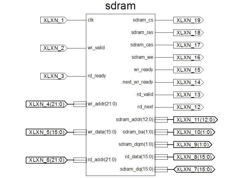
Yes, checking it out. Maybe now I can make some heads and tails of it. I've made a symbol of it to see the I/O's and get a general feel. I see the CPU sends a read & write address A0-A21 (2M), but the SDRAM you used is a 4Mx16. Did you only use half of the RAM?
EDIT:Oops, A0-A21 is 4M.
Symbol: