OT: DIPSY - tiny FPGA allows for 6502 in 8 pin DIP?
OT: DIPSY - tiny FPGA allows for 6502 in 8 pin DIP?
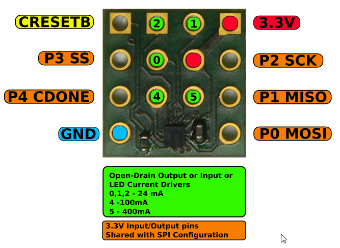
I just love the look of this project: it's footprint compatible with 8 pin DIP, with 5 more I/Os with enough drive for LEDs. Runs at 3.3V, has 7k RAM and a small Lattice FPGA on it. I think it's big enough for a 6502 core, but haven't checked. It offers an SPI interface. And all for about $5 - although right now it seems you have to build your own from the (open) design.


Re: OT: DIPSY - tiny FPGA allows for 6502 in 8 pin DIP?
It's a iCE40UL1K-SWG16 which has 1248 logic cells. I don't know if that's enough to implement a 6502 and the glue? If it is, It would make a nice controller in a system full of SPI peripherals. 
8 bit fun and games: https://www.aslak.net/
Re: OT: DIPSY - tiny FPGA allows for 6502 in 8 pin DIP?
I've had no problems fitting Arlet's 6502 core with peripherals into an XC3S50, which only has 648 slices. I think 'logic cells' are 1/2 slice, so it is about the same. Should not be a problem.
Also, there are 2 built-in i2c ports, pwm and 400mA and 100mA output pins, according to the datasheet.
I am not sure I'd enjoy working with 0.35mm-pitch SMT, however.
Also, there are 2 built-in i2c ports, pwm and 400mA and 100mA output pins, according to the datasheet.
I am not sure I'd enjoy working with 0.35mm-pitch SMT, however.
In theory, there is no difference between theory and practice. In practice, there is. ...Jan van de Snepscheut
Re: OT: DIPSY - tiny FPGA allows for 6502 in 8 pin DIP?
I just got an Icestick board with the same chip. The open-source toolchain is a joy to work with, so far, and FAST! It takes under 10 seconds to build and configure the J1a Forth processor. I will do some more investigation about fitting a 6502...
In theory, there is no difference between theory and practice. In practice, there is. ...Jan van de Snepscheut
Re: OT: DIPSY - tiny FPGA allows for 6502 in 8 pin DIP?
My first attempt to synthesize Arlet's core was a bust - after about 20 seconds of crunching verilog, 17000 LUTs... Something is wrong. ICE40 cells lack some of the XIlinx features - no shift register or RAM capabilities, but it should not be that big.
I'll keep researching as time permits.
I'll keep researching as time permits.
In theory, there is no difference between theory and practice. In practice, there is. ...Jan van de Snepscheut
Re: OT: DIPSY - tiny FPGA allows for 6502 in 8 pin DIP?
Interesting. One of the features of Arlet's core is a small 4x8 ram serving as a register file.
Re: OT: DIPSY - tiny FPGA allows for 6502 in 8 pin DIP?
Registers must be implemented in flops, taking up 32 cells. But given that you generally need a mux in front of a register, the LUTs may be well utilized anyway.
I still think something went wrong during synthesis...
I still think something went wrong during synthesis...
In theory, there is no difference between theory and practice. In practice, there is. ...Jan van de Snepscheut
Re: OT: DIPSY - tiny FPGA allows for 6502 in 8 pin DIP?
I think I had an issue mapping to a block ram, causing a flop-based ram to synthesize. My last attempt is a lot more promising:
862 cells. Reasonable. Just enough room to squeeze in a UART and some IO, I think, although a tight fit.
Code: Select all
   Number of wires:                700
   Number of wire bits:           1017
   Number of public wires:          87
   Number of public wire bits:     345
   Number of memories:               0
   Number of memory bits:            0
   Number of processes:              0
   Number of cells:                862
     SB_CARRY                       29
     SB_DFF                         32
     SB_DFFE                        83
     SB_DFFESR                       7
     SB_DFFESS                       3
     SB_DFFSR                        6
     SB_DFFSS                        1
     SB_LUT4                       700
     SB_RAM40_4K                     1
In theory, there is no difference between theory and practice. In practice, there is. ...Jan van de Snepscheut
Re: OT: DIPSY - tiny FPGA allows for 6502 in 8 pin DIP?
OK, so about three-quarters of the device for the CPU core - not too bad! And 512 bytes of memory, if I'm not mistaken. (Looks like the chip should offer 7k bytes max?)
Re: OT: DIPSY - tiny FPGA allows for 6502 in 8 pin DIP?
Given the limited number of pins, you can't have that many peripherals anyway. So a 6502 with 7K, a serial port and a few PWM pins is a pretty reasonable system.
Now if only Antti would make the board - I don't really want to reflow chips small enough to inhale. Well I kind of do, but not really.
EDIT:
I don't know of any inexpensive PCB manufacturer that offers 3mil traces and really tiny vias... The board is small enough that even an expensive process will be OK (a few hundred boards on a panel...) But the chip does need a few extra parts and placing accuracy of 0.1mm or so.
EDIT:
Also there is the configuration issue. Most ICE40's have a non-volatile configuration PROM (one-time-programmable with special license magic - Lattice advises to contact them about further information, not a good sign for free toolchain). This design gets configuration from an external device (via SPI?), and adding a configuration flash will take up pins and board space, not to mention add to the cost of the board.
In theory, there is no difference between theory and practice. In practice, there is. ...Jan van de Snepscheut
Re: OT: DIPSY - tiny FPGA allows for 6502 in 8 pin DIP?
According to the Lattice iCE40HX data sheets, the OTP configuration ROM appears to external devices as any ordinary SPI flash ROM. It obeys the same command set. The data sheet I have makes no mention of licenses required for programming.
Re: OT: DIPSY - tiny FPGA allows for 6502 in 8 pin DIP?
I hope so! I came across an ominous note on the website saying "if you wish to use the NVCM feature, contact us". Perhaps it's for a factory pre-programmed run; I hope my understanding of this was incorrect and the ROM can be programmed using opensource tools.
I haven't come across any mention of anyone programming the NVCM, other than the generic "you can only do it once" comments.
EDIT: I think you are right: from the horse's mouth:
I haven't come across any mention of anyone programming the NVCM, other than the generic "you can only do it once" comments.
EDIT: I think you are right: from the horse's mouth:
Quote:
The NVCM can be programmed using the Lattice Diamond ® Programmer (version 2.2 or later) or an external
processor.
processor.
In theory, there is no difference between theory and practice. In practice, there is. ...Jan van de Snepscheut