6502.org
http://forum.6502.org/

A 6502 SoC Project using a Spartan 3 FPGA
http://forum.6502.org/viewtopic.php?f=10&t=1730
Page 4 of 15

Author:  ElEctric_EyE [ Fri Jan 14, 2011 11:10 am ]
Post subject: 

Windows XP Pro, 32-bit...

Author:  Arlet [ Fri Jan 14, 2011 11:50 am ]
Post subject: 

I've compiled the bin2coe C program for win32, and put the executable here:

http://ladybug.xs4all.nl/arlet/fpga/source/bin2coe.exe

Open a 'cmd' window in Windows, go to directory with filename.bin file, and enter the command:

bin2coe filename

It will leave a filename.coe next to it.

I tried it on a hello.bin file containing the ASCII text for "hello\n", and I got this hello.coe file:

Code:
MEMORY_INITIALIZATION_RADIX=16;
MEMORY_INITIALIZATION_VECTOR=
68,65,6c,6c,6f,0a,

Author:  ElEctric_EyE [ Fri Jan 14, 2011 11:15 pm ]
Post subject: 

Excellent. Thank you very much! Will try to make the ROM again tonight. In the next few days I should have some postable results...

When I was using discrete components (i.e. EEPROM, SRAM, CPU), I was compensating for the slow EEPROM, by copying the "OS" from EEPROM to SRAM so the cpu could run as fast as possible.

The past couple days I started to realize, by having the "OS" in an internal FPGA "ROM", there will be no need to do the previous copy operation. Which got me thinking even further, the RAM the 6502 sees should be internal to the FPGA where the 6502 core is as well. Then the memory window into the SD card which is external to the core, could use my proven phase 2 switching scheme to accomodate the slower access speeds. I don't know if this makes sense to anyone, but it does to me. I will explain as this develops.

Wish I had even more time on the days I work...

------------------------------------------------------------------------------
Now that I think about it... I think I have downloaded that program when I googled .coe converters. I got it from edaboard.com. I didn't like the command line entry...

I am looking for a "all in one" hex editor. One that can edit multiple file types, etc. and put comma delimiters in the final saved version, all in one program... I'm just going to break down and buy it!

So far I am using M. Kowalski's assembler for program data, HxD hex editor for font/program data merging, then I would have to use a .coe converter program...

If I could just use 2 programs to present to ISim a necessary .coe file for ROM generation, I would be very happy! Call me lazy? efficient? (I've always had a problem distinguishing!)

Author:  ElEctric_EyE [ Mon Jan 17, 2011 12:08 am ]
Post subject: 

Arlet wrote:
I've compiled the bin2coe C program for win32, and put the executable here:

http://ladybug.xs4all.nl/arlet/fpga/source/bin2coe.exe

Open a 'cmd' window in Windows, go to directory with filename.bin file, and enter the command:

bin2coe filename

It will leave a filename.coe next to it.

I tried it on a hello.bin file containing the ASCII text for "hello\n", and I got this hello.coe file:

Code:
MEMORY_INITIALIZATION_RADIX=16;
MEMORY_INITIALIZATION_VECTOR=
68,65,6c,6c,6f,0a,


I've done the same (not bragging, just questioning syntax) with HHD. But I'm having problems implementing the .coe file...
I used HHD to make a file (it was smaller than 4096 bytes though), that looked like yours above, in addition, it had the semicolon at the very end, but it gets stuck when I point ISim to the coe file when creating the ROM.

When specifying the size of the ROM, does the coe file have to be an exact fit?

I notice the syntax according to the Xilinx example has each data on its own line, followed by the comma, and the carriage return?. Maybe we are not following spec here... Will continue experimenting!

BTW, when I said I found the bin2coe file on edaboard, I was mistaken. I had found a hex2coe converter there. Re-Testing...

Author:  Arlet [ Mon Jan 17, 2011 5:23 am ]
Post subject: 

I don't know. I've never used the .coe file mechanism, or the core generator myself.

What do you mean by "it gets stuck" ?

Author:  ElEctric_EyE [ Mon Jan 17, 2011 1:23 pm ]
Post subject: 

hex2coe does not work correctly with the intel hex file M.Kowalski's assembler generates. It just spit out all zero's.

bin2coe does generate a file in the form you pasted above (looking at it in notepad) with the correct data. I just had to rename the .65b (binary image) from MK's assembler to .bin and that part worked, but...

In the IP_Core Generator, when it's creating the "ROM".xco file, the HDL analysis has been running now for 15 min's, which seems to be too long. Even on a 2.8GHz Pentium 3 laptop w/2GB RAM.

I'm letting it run, because it's doing something, slowing the system and the HDD light flashes every few seconds...

Tomorrow on my day off I'll try it on a more capable E8500.

Arlet is there any way to modify bin2coe to generate the string in a single column, then a semicolon at the very end?

25 minutes now, still on HDL analysis...

Author:  Arlet [ Mon Jan 17, 2011 1:32 pm ]
Post subject: 

New bin2coe.exe here:

http://ladybug.xs4all.nl/arlet/fpga/source/bin2coe.exe

Btw, if you don't supply a .coe file at all, does the synthesis take this long too ?

Is there an option to check whether you want block RAM or distributed RAM ? If so, you need to make sure it uses block RAM.

Author:  ElEctric_EyE [ Tue Jan 18, 2011 2:54 am ]
Post subject:  is

That new .COE generator is Top-Notch M8! :o. I had to test it first. It generates a .COE file 100% according to Xilinx spec as far as I can tell...

I hope I'm not in the wrong here now, after you have done so much work, because I have been using distributed RAM... In answer to your questions: The synth takes no time at all making a ROM with no COE file selected, and there is a selection for Block RAM or Distributed Ram...Testing...
--------------------------------------------------------------------------------------
Same result after creating a new project with the 4Kx8 distributed RAM...

For giggles, I specified a much smaller 16bx8 distributed RAM in another new project (so as not to confuse ISE, even rebooted PC and deleted old projects) and it synth'd in under a minute! So preliminary tests suggest either I did/am doing something wrong, an ISE program bug, or this laptop is way to slow. I would bet on the last... Will find out tomorrow on 3.16GHz E8500 system early in the morning.
Author:  Arlet [ Tue Jan 18, 2011 5:30 am ]
Post subject: 

What I don't understand is that it would take longer if you specify the initial contents of the ROM. The synthesis and place & route should be exactly the same, no matter what you decide to put in the ROM.

Well, if everything fails you can still use the method I suggested earlier, using verilog code for the ROM instead of using the core generator.

Quote:
I have been using distributed RAM


Big distributed RAM is going to be slow in synthesis, so that makes sense. It uses individual LUTs as 16x1 bit RAM devices, and it's going to combine 2048 of them to make a 4KB ROM, plus a bunch more for decoding.

Block RAM should be fast and simple though.

Author:  ElEctric_EyE [ Tue Jan 18, 2011 2:06 pm ]
Post subject: 

Ok, using the Block Ram CoreGen pointed out a problem. The .bin file I was converting was 8K not 4K! This is what happens when I try to do stuff after a long day at work. In addition I was attempting to use distributed RAM. I missed the part about 16x1 memories in the Distributed Memory Generator data sheet. FYI, it took <2min's on the laptop to fit the .COE file into the 4Kx8 ROM.
Arlet, Thank you for your patience and the converter program!

I think it's time to arrange the board...

I can see already my simple block diagram, may become even simpler. Fitting an entire 64K of RAM for the 6502 core, inside the Spartan 3, must be possible...No need for the external 10ns SRAM, no need for the external 512Kx8 EEPROM. But I think, in addition to the SD Card, I should have a 2Mx8 Flash I've had my eye on for awhile now. The fast 6502core can slow down to copy routines/data from the 70ns Flash into the core, then speed back up again. Can't wait to see the top speed!

Next step, after layout/final ideas, is wire wrapping. Then I'll fit the 6502 core, ROM and RAM for $0000-$01FF (the test), and hook it up the display I have currently in the PWA project (the proof).

Author:  ElEctric_EyE [ Wed Jan 19, 2011 12:02 am ]
Post subject: 

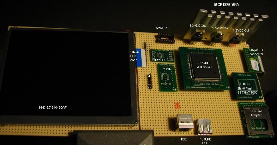
The PS2/FUTURE(USB) and VR's are in place and can't be moved. Most of the IC's are optimally placed at this point but can be rearranged. I put the XC3S400 closest to the Voltage Regulators, even though it only takes 200mA max quiescent...

Image

Notice the NHD Display can easily be removed and put back into the PWA Project...

Next I wire in bypass cap's after I reread this Xilinx AppNote. I've used .1uF in the past with no problem with the Spartan 2 100-pin QFP running @80MHz, but I must be sure...

Author:  Xor [ Wed Jan 19, 2011 4:37 am ]
Post subject: 

Hey, just wanted to pop in here and let you know this is an awesome project!

I work in Verilog all day long for my job :P I've always wanted to dig into building out actual hardware around an FPGA, but just haven't had the time or money to learn it all up.

So, it's cool to see your project with a custom design based around an FPGA.

Anyway, keep up the good work!

Author:  Arlet [ Wed Jan 19, 2011 10:05 am ]
Post subject: 

@EE: did you run a simulation as well, to see if the 6502 core would run the program in your memory ?

Author:  ElEctric_EyE [ Wed Jan 19, 2011 1:03 pm ]
Post subject: 

Xor wrote:
Hey, just wanted to pop in here and let you know this is an awesome project!

I work in Verilog all day long for my job :P I've always wanted to dig into building out actual hardware around an FPGA, but just haven't had the time or money to learn it all up.

So, it's cool to see your project with a custom design based around an FPGA.

Anyway, keep up the good work!


Thanks for the moto! Sounds like you're well along on your own project, making very quick progress that's for sure. I'm more of a tinkerer, although I'd prefer to be called a troubleshooter. That's what I do as an auto technician. Anyway, drop in any time!

Arlet wrote:
@EE: did you run a simulation as well, to see if the 6502 core would run the program in your memory ?


I've never run a simulation, is it difficult?
I was just going to do the top-level schematic using your core, the 4KROM and some RAM for the stack and 0-page, some simple address decoding, wire it up to the display and throw the switch. I don't even need the I2C core yet, because the DS1085L default output is 48MHz. So not too much wiring :lol: . That's a beautiful thing.

Author:  Arlet [ Wed Jan 19, 2011 1:22 pm ]
Post subject: 

Simulating isn't particularly difficult, especially in this case, because you don't really need any test bench to get started. ETA: well, you need to generate a clock signal, and a reset pulse.

Simulations are very helpful, because you can use a waveform viewer to see every signal inside the model, such as internal 6502 registers, buses, and other internal signals. For complex hardware designs, a simulation can save tons of debugging time, especially with FPGAs were you can't just stick a scope probe on an internal signal. Some vendors offer free verilog models of their chips, so you can put those in the simulation as well. I've used some Micron SDRAM models, for instance.

The only thing is that I don't really have experience with the Xilinx simulation tools. I'm using 3rd party verilog simulation software and waveform viewers.

Page 4 of 15 All times are UTC
Powered by phpBB® Forum Software © phpBB Group
http://www.phpbb.com/