6502.org Forum  Projects  Code  Documents  Tools  Forum
It is currently Fri May 10, 2024 2:03 pm

All times are UTC


Post new topic Reply to topic  [ 44 posts ]  Go to page Previous  1, 2, 3
Author Message
PostPosted: Fri Jul 07, 2023 5:35 pm 
Offline
User avatar

Joined: Tue Nov 16, 2010 8:00 am
Posts: 2353
Location: Gouda, The Netherlands
GARTHWILSON wrote:
Arlet wrote:
In my understanding, a fill is simply a big polygon filled with copper that's connected to a specific net. In the case of ground fills, it's usually the same shape as the board outline.

That's a ground plane.  By "fills" or "pours," we're talking about filling smaller blank areas here and there on the board, which is usually done by people who think it's about electrostatic shielding and don't understand the matter of mutual inductance and a ground return that needs to be continuous under the signal trace it's returning the current for, for the entire length, without interruptions or detours.


Ok, so using that terminology, I always put two ground planes on my double sided boards.


Top
 Profile  
Reply with quote  
PostPosted: Fri Jul 07, 2023 7:46 pm 
Offline

Joined: Mon Jan 19, 2004 12:49 pm
Posts: 683
Location: Potsdam, DE
I just forked out fifteen euros for a second hand toaster oven... it may have been a mistake. I tested it by executing some toast in it, and on turning on the lights in the cellar, popped the lighting circuit for each room in the cellar. Problem is, it only pops when the lights in the cellar are on, and it was plugged into the ground floor power circuit.

Still thinking this one through!

Neil


Top
 Profile  
Reply with quote  
PostPosted: Wed Jul 12, 2023 11:27 pm 
Offline

Joined: Sat Oct 09, 2021 11:21 am
Posts: 704
Location: Texas
So much learning!

Attached are some pictures. I have learned so much about solder SMT stuff! Here's a small list:

1) Those 0805/2012 resistors and capacitors are WAY TINY! I'll be going with bigger ones in the future.

2) Film resistors are really flat! I like them standing up higher.

3) SOIC chips are a piece of cake. I had some solder bridges here and there, but it was easily fixed with either a super hot soldering iron or some solder wick.

4) Less solder is more effective. You only need a *tiny* amount for each pin. I wasn't used to that.

5) The special tweezers I got for this were bent within a half hour. I don't know if I'm just not used to them, or if they were not great quality or something, but yeah, I'll have to figure something else out in the future.

6) I had a little headlamp+magnifier, and wow, that was super important for that CPLD. I used that nearly the entire time, until I got to the through-hole stuff of course.

7) The SRAM chip had a wider spec than what KiCad supplied, and I am thankful I made those pads longer! It barely fit even after I doubled each pad's width!

8 ) Those SMD oscillators seem easy enough, and they are, but the pads from KiCad were basically meant for stencil + paste. Oh that was so annoying! Things you just don't think about, I guess.

9) That TQFP-44 CPLD was a PAIN!!! I would bridge the pins almost automatically. The solder wick helped a lot, and that was my main method of removing it. BUT, before I got wise, I was stupid, and ripped off one of the corner pins, as well as break a trace on the board. Oh, SO annoying! That tiny bodge was a 1 hour ordeal. I actually *threw* the board once because it was just so difficult. But then I picked it up and kept going :) I want to practice more on those and get better with the solder wick method. I was hoping my soldering iron was hot enough to just melt the access away, drip it off using gravity. That was NOT the case, my soldering iron apparently just doesn't get hot enough for that, or maybe I need an even more fine-tip soldering iron tip. [ You can see my tiny blue bodge wire in the top-down picture. ]

10) I had fun learning. And that's important!

So, this tiny little board took 4 hours, mainly on the CPLD and those tiny resistors and capacitors. Every through-hole component was like a reward for all the pain I had with everything else.

My future in SMT land is just beginning, but I'm definitely going to consider a bake/skillet method for that CPLD. It would save a lot of time and issues. The rest are totally doable by hand as long as you get the right parts and pads.

I'll be posting more about my 6502 code monitor/editor on it's original post, here:

viewtopic.php?f=4&t=7642

It worked the first time!!! Thanks everyone! :)

Chad


Attachments:
20230712_181052.jpg
20230712_181052.jpg [ 1.95 MiB | Viewed 6872 times ]
20230712_181101.jpg
20230712_181101.jpg [ 2.38 MiB | Viewed 6872 times ]
20230712_180801.jpg
20230712_180801.jpg [ 2.27 MiB | Viewed 6872 times ]
Top
 Profile  
Reply with quote  
PostPosted: Thu Jul 13, 2023 1:47 am 
Offline

Joined: Fri Dec 21, 2018 1:05 am
Posts: 1076
Location: Albuquerque NM USA
You should use even less solder. The SMT solder joints should not buldge out like convex joints. You should strive for concave joints (like joints on mortar brick wall). Of course the important thing is get it to work which you did. Concave/convex joints are about how well they handle thermal/mechanical stress and long term reliability--not important for now, other than snide remarks from old timers like myself.

Get another fine tweezers and cut the bent tips from the current tweezers so it can handle greater force such as straighten out bent leads. You'll likely go through a few pairs of tweezers before you learn its limitation.

You will develop a favorite orientation of component leads with respect to solder tip and solder. So constantly rotate your board to that favorite orientation as you work.

Use the smallest diameter solder you can find. 10 mil (0.25mm) is ideal, but it is hard to find.

Learn how to use 0805 components. It is a perfect fit between two leads 0.1" inch apart. I use 0805 frequently for engineering changes and design modifications.

TQFP44 is 0.8mm spacing which is generous for SMT. You'll encounter 0.65mm and 0.5mm later which will be more challenging. Garth has mentioned drag soldering for fine pitch components. It does work, but you need regular practice to be good at it.

You've mentioned magnifier and light. Wait until you eventually tried a stereo inspection microscope! here is a talking point for inspection microscope: it is a great education tool--kids can learn so much looking at things under the microscope. So can you, and oh yea, it is good for SMT soldering, too.
:wink:
Bill


Top
 Profile  
Reply with quote  
PostPosted: Thu Jul 13, 2023 3:44 am 
Offline
User avatar

Joined: Tue Nov 16, 2010 8:00 am
Posts: 2353
Location: Gouda, The Netherlands
To make neat soldering easier, I highly recommend Loctite Crystal 511. It's such a joy to work with.


Top
 Profile  
Reply with quote  
PostPosted: Thu Jul 13, 2023 10:40 am 
Offline

Joined: Mon Jan 19, 2004 12:49 pm
Posts: 683
Location: Potsdam, DE
I have been playing with solder paste and a hot air blower this week (the toaster oven I intended to use trips the circuit breaker when it gets warm, so further investigation required there!) and concluded that I will automatically include a stencil with my next pcb order. Even with the syringe it is way too easy to apply way too much solder to the joint - and I'm working with 0.65 and 0.5mm spacing, plus 0603 which is the smallest passive I can comfortably manage.

The TPS62172DSGR (https://www.digikey.de/en/products/deta ... GR/2833456 ) comes in a minuscule and horrible WFDN8 package with a pad which must also be soldered; it is less than easy to fit at 2mm square...

My previous approach was to tin the pcb contact with the minimum solder possible (still often too much), slather with no-wash flux, apply the components one at a time and use the hot air blower on 400C and the minimum airflow to avoid having to play hunt-the-component...

Neil


Top
 Profile  
Reply with quote  
PostPosted: Thu Jul 13, 2023 7:20 pm 
Offline

Joined: Sun May 13, 2018 5:49 pm
Posts: 247
First of all, congratulations on diving right in and coming out the other side with a working board! As you've already discovered, most mistakes you might make are fixable and you now have an appreciation and understanding of some of the techniques used to fix these issues so they won't be as scary on your next board.

I do see one component that may not be fully soldered - if you haven't found it already, you should check the 10K right over the "KMR2 SPST" RESET switch (not populated). I don't see a meniscus up to the left end resistor.

sburrow wrote:
1) Those 0805/2012 resistors and capacitors are WAY TINY! I'll be going with bigger ones in the future.
0805 is the "larger" size in my work, but I make circuits that need to fit in very small spaces. By all means, order a size that you are comfortable with.

sburrow wrote:
4) Less solder is more effective. You only need a *tiny* amount for each pin. I wasn't used to that.
Yes, it's tiny solder for tiny parts. Using a stencil helps with that as it puts the right amount for each pin. I use 0.015" solder for most of my SMD work when hand soldering.

sburrow wrote:
5) The special tweezers I got for this were bent within a half hour. I don't know if I'm just not used to them, or if they were not great quality or something, but yeah, I'll have to figure something else out in the future.
The most important thing is to never push, prod, or pry with them with any kind of force. When you are used to working with pliers, where you do all of those things, it can take some getting used to. If it's going to bend a piece of thin wire, it's too much force. I recommend getting a cheap set of stainless steel picks (eg. dental picks) for all of your poking, scratching, and prying needs.

sburrow wrote:
6) I had a little headlamp+magnifier, and wow, that was super important for that CPLD. I used that nearly the entire time, until I got to the through-hole stuff of course.
You don't need to stop using magnification for through hole work (assuming your setup is comfortable and your focal range is reasonable so you don't have to hunch over) - it makes that work much easier as well because you can watch the solder flow and get a perfect joint every time. If you see yourself doing a lot of this, I would recommend you at least consider a stereo inspection microscope. It's way better than the head mounted magnifiers, but it's also an order of magnitude more expensive.

sburrow wrote:
7) The SRAM chip had a wider spec than what KiCad supplied, and I am thankful I made those pads longer! It barely fit even after I doubled each pad's width!
When using parts I've never used before, I will often print (on paper) a 1:1 copy of my board and physically place the parts on the paper to make sure I haven't missed anything. Of course, that only works if you have the parts already. Also, it is possible to put "wide" SOIC parts on narrow SOIC pads with a bit of extra work:
Attachment:
File comment: Wide SOIC soldered to narrow SOIC pads at an angle
3d_soldering.png
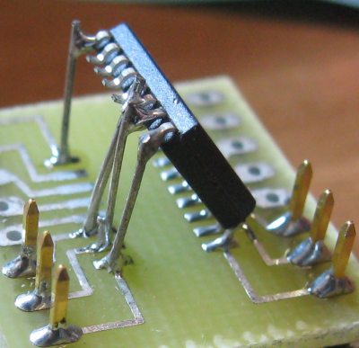
3d_soldering.png [ 1.06 MiB | Viewed 6802 times ]


sburrow wrote:
9) That TQFP-44 CPLD was a PAIN!!! I would bridge the pins almost automatically. The solder wick helped a lot, and that was my main method of removing it. BUT, before I got wise, I was stupid, and ripped off one of the corner pins, as well as break a trace on the board. Oh, SO annoying! That tiny bodge was a 1 hour ordeal. I actually *threw* the board once because it was just so difficult. But then I picked it up and kept going :) I want to practice more on those and get better with the solder wick method. I was hoping my soldering iron was hot enough to just melt the access away, drip it off using gravity. That was NOT the case, my soldering iron apparently just doesn't get hot enough for that, or maybe I need an even more fine-tip soldering iron tip. [ You can see my tiny blue bodge wire in the top-down picture. ]
These will simply take practice, and you've already completed practice session #1. After a while, this pitch will be easy and you'll be cursing at even finer pitch parts with even more legs to get solder bridges on. Also, it may be comforting to know that even those of us who do this work for a living have all of these exact same issues. It's more important to know how to fix a solder bridge so that, when it inevitably happens, you don't worry about it and just fix it.

Your bodge looks reasonable. For hobby work, you just need to get the things that should be touching to be touching and keep the things that shouldn't be touching from touching.

sburrow wrote:
My future in SMT land is just beginning, but I'm definitely going to consider a bake/skillet method for that CPLD. It would save a lot of time and issues. The rest are totally doable by hand as long as you get the right parts and pads.
Once you get to that stage, you'll find its faster to just place all of the passives while the board is already pasted and then after reflow it's all done*

* after you fix the shorts and the parts that shifted wrong and the parts that tombstoned....

Your adventures up to this point will still be worth the hassle, as you are still going to have to fix shorts and open circuits - you just will have less of them to deal with if your reflow process goes well. I do recommend getting a good flux and using it when battling shorts - it will help the solder flow back to the places it's supposed to be.

I use SMD291 from ChipQuik (not sponsored) because you can dispense to just a single IC leg (it comes in a syringe), it stays where you put it, it cleans up with isopropyl alcohol (not all fluxes react well to IPA), and it lasts for over 2 years without refridgeration so you can just leave it on your bench next to your iron. I give the syringe a tiny squeeze until a little comes out the tip, and then a dab it where I want it. For SMD work, you don't need much but you should have some flux if you are reheating a joint (will help prevent that "solder icicle" you get when you pull the iron away).

Unless you go gung-ho, even the smaller 5cc syringe (part# SMD291NL) should last a long time and might be a good start (if you don't already have flux) to see if you like it. Also, check your desoldering wick and make sure it has flux in it. If it doesn't say something like "Rosin" or "No-Clean" on it, then you should be adding flux when you use it.


Top
 Profile  
Reply with quote  
PostPosted: Fri Jul 14, 2023 12:56 pm 
Offline

Joined: Sat Oct 09, 2021 11:21 am
Posts: 704
Location: Texas
Thank you all, I appreciate the help and advice.

SamCoVT wrote:
I do see one component that may not be fully soldered - if you haven't found it already, you should check the 10K right over the "KMR2 SPST" RESET switch (not populated). I don't see a meniscus up to the left end resistor.


I don't know how you did that, but you were right! I just solder it better-ish. Thank you, and, uh, wow. You are definitely the professional!

SamCoVT wrote:
0805 is the "larger" size in my work,


Haha!

SamCoVT wrote:
Also, it is possible to put "wide" SOIC parts on narrow SOIC pads with a bit of extra work:


That's funny :)

SamCoVT wrote:
If it doesn't say something like "Rosin" or "No-Clean" on it, then you should be adding flux when you use it.


I actually just ordered a stencil and some "no clean" lead based paste on Amazon, will try it out on a second board next week. Thank you for all of the advice and help, that is very beneficial!

barnacle wrote:
I will automatically include a stencil with my next pcb order.


That's my plan too. Eventually I want to do the entire board like that, minus any through-hole style connectors.

plasmo wrote:
Get another fine tweezers and cut the bent tips from the current tweezers so it can handle greater force such as straighten out bent leads. You'll likely go through a few pairs of tweezers before you learn its limitation.


It is a learning process for sure. Will keep at it.

plasmo wrote:
here is a talking point for inspection microscope: it is a great education tool--kids can learn so much looking at things under the microscope. So can you, and oh yea, it is good for SMT soldering, too.


Something to convince the wife? :) She's already giving me "that look" when I said I'd like to put my board in one of *her* skillets on *her* stove top.

Thank you everyone! Lots of learning!

Chad


Top
 Profile  
Reply with quote  
PostPosted: Fri Jul 14, 2023 3:12 pm 
Offline

Joined: Sun May 13, 2018 5:49 pm
Posts: 247
sburrow wrote:
She's already giving me "that look" when I said I'd like to put my board in one of *her* skillets on *her* stove top.
That would be a big mistake (for multiple reasons, but "the look" is by far the most serious). You should keep an eye out for cheap skillets and single-burner hot plates (for cooking). Avoid the aluminum skillets (if possible) as they warp the worst and it's best if your board sits flat against the skillet; it will work reasonably well even with an imperfect (non-flat) setup, though, and the aluminum pans usually at least start out flat (and can be "adjusted" with a rubber mallet (when cold) if they don't sit flat).

The first reflow you do is somewhat magical as the surface tension of the solder will move the parts into alignment on their pads. You just need to place them so they are more than 50% on the correct pads and not touching other pads - don't waste time trying to get them perfect, as the reflow will often fix it for you. Just watch the board until all solder joints have reflowed (turned into molten solder - they get shiny when this happens). You can quickly nudge parts that didn't flow quite right while everything is molten, but you should get it all done in less than a minute or two once the solder starts to melt (if possible). Then remove skillet from heat and (patiently) let it cool and it will look like it was soldered by a pro. You may still need to fix a solder bridge or a connection that didn't flow properly, but you'll usually have a lot less of those than you would get by hand soldering.

The solder melts at around 220C (lower for leaded), which isn't that hot for a cooking burner, so use the lowest burner setting that works well and brings the board up to melting temperatures in 2 to 5 minutes. Any faster than that and you risk overshooting the max temperature the components can handle, and any slower than that and you will use up all of the flux before you actually melt the solder. The latter is a better issue to have, as you can add flux and touch-up with an iron any connections that didn't wet or flow properly.

sburrow wrote:
Eventually I want to do the entire board like that, minus any through-hole style connectors.

Once you start going to Surface Mount Technology (SMT), you'll find that many of the connectors are available in SMT as well. Those are the only components I recommend spending the extra time to get well aligned on their pads before reflow. SMT connectors are easier to mechanically damage (rip off the board) as they are soldered to the copper foil and that foil is only glued to the PCB material. If you need mechanical ruggedness (eg. screw terminals for wires that might be tugged on) then stick with through-hole.


Top
 Profile  
Reply with quote  
PostPosted: Fri Aug 04, 2023 12:44 am 
Offline

Joined: Sat Oct 09, 2021 11:21 am
Posts: 704
Location: Texas
SamCoVT wrote:
... remove skillet from heat and (patiently) let it cool and it will look like it was soldered by a pro. You may still need to fix a solder bridge or a connection that didn't flow properly, but you'll usually have a lot less of those than you would get by hand soldering.


Yep! Perfect, just like you said, thank you Sam. I was re-playing your post in my mind while doing the whole procedure, and attached is a picture of the outcome! Here are the steps in brief, just so others will know:

1) I got a thin steel stencil for the QFP-44 10x10mm part matching my Xilinx CPLD XC9572XL part. I also got "no clean" leaded solder paste with a melting point of around 360 degrees Fahrenheit. I put the solder paste in the refrigerator until I was ready to use it.

2) I taped the stencil down to the board with painters tape, made sure it would be easy to remove without shifting things.

3) I applied a tiny amount of paste on all of the stencil holes, then wiped it around with an old plastic card. I think I didn't apply enough, so I did more and made sure it was all filled in as much as it could hold. It didn't *look* filled in completely, but it was fine. Some paste got on the board itself, so I wiped it off with a paper towel. Also, the stencil had extra long pad holes, but my KiCad pads were shorter. So basically I had paste on the soldermask, but apparently that didn't matter in the end.

4) I removed the stencil by removing one side of the tape, then rotated the stencil up away from the board. It either shifted some or the paste melted a bit, because it looked like it was generally one big blob with indents, kind of.

5) I took fine tweezers and put the CPLD where it should be. I got it almost right on the first try, but I did have to shift it a tiny bit. Again, it looked like it was just sitting in a blob of paste, I don't think I was looking at soldermask between pins at this point.

6) I put an unfolded piece of aluminum foil on a single burner on our glass-top stove. I had tested temperatures beforehand with a cooking thermometer directly on the burner surface, and so I knew where to turn the knob before hand. I was wanting it to reach the 360 degrees and then just past, and that was about half-way for me.

7) The board was heating up pretty quickly, so I slightly adjusted the knob for the burner. Then I cranked it up to my preset position (half-way), and watched it while keeping the cooking thermometer nearby. I was wondering if the board wasn't sitting fully on the burner, so I went to get a butter knife to press on the board. When I came back, the solder was already melting. Within literally 3 to 5 seconds or so it looked perfect.

8 ) I pulled the foil+board from the burner, and turned it off. I let the board sit for a bit. I noticed that there was a *tiny* bridge between two pins. After cooling for a minute, I tested it with the multimeter and yes it was a bridge.

9) I heated up the soldering iron to the hottest I could get it. I then touched the soldering iron tip to the pins that had the bridge and... poof it was gone! Yep, I didn't even use solderwick, it just disappeared :)

10) I thought I saw one pin that didn't have enough solder (unlikely, but whatever), so I touched it with the soldering iron too and it seemed to be fine, I think.

So! The hardest part for me to hand solder is no longer the hardest part at all! Golly, if I did this for ALL of my SMD parts, that would make things super fast and super easy! I used hardly any solder paste while doing this, it was all done in less than 5 minutes, and it looks professional.

Tomorrow I'm going to solder everything else by hand. Will make a topic about the board itself soon.

Thank you everyone, and thank you Sam in particular. That went so well, I am very pleased by the results! :)

Chad


Attachments:
20230803_191402.jpg
20230803_191402.jpg [ 1.78 MiB | Viewed 6657 times ]
Top
 Profile  
Reply with quote  
PostPosted: Fri Aug 04, 2023 7:30 pm 
Offline

Joined: Mon Jan 19, 2004 12:49 pm
Posts: 683
Location: Potsdam, DE
A little more practice Chad and you'll be doing things like this in your sleep... U2 is 2mm square, has eight concealed pins and a required ninth pad underneath. It was a stinker the first few times, but solder paste with flux and cautious hot air sorted it. It throws out half an amp at 3.3v from up to 17v input :mrgreen:

Attachment:
1691177111501.jpg
1691177111501.jpg [ 3 MiB | Viewed 6605 times ]


Neil


Top
 Profile  
Reply with quote  
PostPosted: Sun Aug 06, 2023 9:37 pm 
Offline

Joined: Sun May 13, 2018 5:49 pm
Posts: 247
Excellent work. I'm glad it worked out so well for you. It does take more prep. time, but vastly makes up for it in doing all the solder joints at once.

Regarding the stencil apertures (openings) that are larger than your pads, that's called overprinting and it's a valid technique for getting more solder into a joint. It's often used for connectors to create a better mechanical connection. If it works well, the extra solder will be drawn towards the pad. If it doesn't work well, you end up with solderballs that aren't connected to anything. In your case, it's likely just a mismatch between the pad sizes KiCad uses and the stencil design. Longer pads on QFPs (Quad Flat Package) used to be more common, and they are much easier to hand solder, but now most manufacturers are recommending the minimum size for pads so you can cram more parts on a small board.

Watch out for solderballs - if they are loose, you should remove them from the board so they don't end up between pins and short things out. If they are trapped in no-clean flux residue, aren't going to move, and aren't shorting anything (electrical clearances are OK), then you can leave them. You can get them even when not overprinting, if some solderpaste ends up on the soldermask and not on a pad. Paste can be messy, so this is definitely something that happens.

It's fine to get stencils for just the hard ICs and stencil them individually, but the next level is to do all the passives as well and you'll need a stencil for your entire board. Depending on what you have available, your options include:
  • Buy a stencil (OSH Stencils has very reasonable prices - I recommend their 5-mil mylar stencils for the kinds of parts you are currently working with)
  • Cutting stencils in plastic (mylar - usually clear or orange, 0.003 to 0.006" thick) with a laser cutter
  • Cutting stencils in metal with a milling machine or router - I've used 0.005" brass shim stock from McMaster (their 8"x12" is a convenient size) with a V-bit
  • Cutting stencils by hand with an x-acto knife - can't recommend for QFPs (Quad Flat Pack) and the like, but I have done this for very simple boards with SOICs (Small Outline Intergrated Circuit) and larger.

Your plastic card is likely fine for use as a squeegee.

Your setup for holding your stencil sounds reasonable. If I'm making more than one board, I tape some scrap boards that are the same thickness as my board to the table so they tightly touch/hold my board on three sides. Make sure the tape is only on the outside of the scrap boards, so there is no "bump" under the stencil at the edges of your board. This provides flat support for the stencil if you have apertures near the edge of the board. The stencil is lined up with the board and a single long piece of tape at the top make a hinge of sorts. Always use the squeegee away from the hinge so the stencil doesn't move. Once your board is pasted, lift the stencil away from the board, replace the board, and the stencil should be aligned or very close to it for the next board. The open side is how you get boards in/out.

A well pasted board will have clean deposits of paste on the pads that don't touch each other. If your board has soldermask, then you can often get away with a less clean print, and if you are prepared to fix any solder bridges then that is plenty good enough. For hobby work, it's more important that every pad have solder paste on it than it is to get a perfect print. The "blobby" result you describe can be cause by the stencil moving, the stencil not being flat against the board (eg. some solder paste made it under the stencil and spread), or by printing (squeegee-ing) more than once. It's a bit of game to get it done in as few passes as possible.

I usually put extra paste on my squeegee and try to paste in as few passes as possible (1 is ideal). If there is a lot of paste on the top surface of the stencil, I pass over the board again with the squeegee vertical to scrape off the excess. In this way, the stencil thickness controls how much solder each joint gets.

If you want to re-use your stencil later, make sure your clean it. I put down a paper towel and place the stencil on that. Then I use a dollar-store spray bottle with IPA (Isopropyl Alcohol - also available at my dollar store but get the 90% stuff, not the 70% stuff) and spray into the apertures and any paste residue, then wipe on top with another paper towel. Flip the stencil and repeat. Inspect to make sure there isn't any paste left in the apertures and repeat as necessary. If the paste has dried into the stencil (because you forgot to clean it right after you used it), a toothbrush (that you aren't ever going to put into a mouth again) works well with the IPA.

The more you do this, the more you'll get a feel for what makes a good print. The good news is that you can do a lot of stuff wrong and still have it come out OK, so just get it "good enough" and carry on. Unless you've melted a part or broken a leg off an IC, almost everything that could go wrong is fixable.


Top
 Profile  
Reply with quote  
PostPosted: Sun Aug 06, 2023 10:23 pm 
Offline

Joined: Fri Dec 21, 2018 1:05 am
Posts: 1076
Location: Albuquerque NM USA
Great write up, lots of real life experiences in those words! What I read between the lines are inspection, inspection, and more visual inspection.

I solder SMT by hand under microscope, it does take more time to do the actual soldering but it requires less setup and clean up. I will stay with that for hobby works.
Bill


Top
 Profile  
Reply with quote  
PostPosted: Mon Aug 07, 2023 6:28 pm 
Offline

Joined: Sun May 13, 2018 5:49 pm
Posts: 247
plasmo wrote:
What I read between the lines are inspection, inspection, and more visual inspection.
That pretty much sums it up. Do it, then look at it, then decide if it's good enough. Too many people skip the looking at it part and proceed directly to power it up.

Here's a summary of my process in photos (slightly photoshopped (GIMPed) to remove identifying information):

Attachment:
File comment: Stenciling Setup
paste1.JPG
paste1.JPG [ 1.21 MiB | Viewed 6517 times ]

This is my setup. The little purple PCB is the one to be pasted. The scrap boards just need to be the same thickness - I keep them around for this kind of use. The stencil (clear 0.005" thick mylar cut on a laser cutter) is aligned. The long piece of tape at the top forms a hinge for the stencil. Because I have apertures (openings) right next to the edge of the board, I probably should have placed a second purple board to the right of the one I am pasting for squeegee support, but I didn't.

Attachment:
File comment: Pasted
paste2.JPG
paste2.JPG [ 542.75 KiB | Viewed 6517 times ]

This is the board pasted with a single squeegee pass (squeegeeing away from the tape hinge). You can see I didn't completely fill the inductor pad in the top left and a few pads in the lower right. I chose not to do a second pass because that risks messing up the good pads and I have at least 50% paste on the pads. Almost everything with work fine if it's at least 50% good enough.

Attachment:
File comment: Stencil Lifted
paste3.JPG
paste3.JPG [ 851.78 KiB | Viewed 6517 times ]

The stencil has to be lifted carefully to avoid smearing the print - no side to side motion.

Attachment:
File comment: Paste Inspection
paste4.JPG
paste4.JPG [ 159.35 KiB | Viewed 6517 times ]

Inspect. Once you've lifted the stencil, you are likely going to make a mess if you try to put it back down, and it might be better to clean the entire board with IPA (Isopropyl Alcohol) and print it again. Cleaning the board has it's own downsides, as you are likely to get solderpaste into the through-holes and that will make stuffing wires or components into those holes difficult later. Best to get it good enough before lifting the stencil.

Attachment:
File comment: Stencil Cleanup
paste5.JPG
paste5.JPG [ 1.43 MiB | Viewed 6517 times ]

Stencil cleaning setup. I spray into the apertures and onto the residual solderpaste, then wipe with another paper towel.

Attachment:
File comment: Finished PCB
paste6.JPG
paste6.JPG [ 319.52 KiB | Viewed 6517 times ]

Completed board (not the one that was just pasted, but it's the same circuit). This board was hand-placed with tweezers. This is lead-free solder (SAC305 alloy with no-clean flux), which has a grainy finish, so you have to look at the shape of the joints rather than if they are shiny or not. Inspection shows that I don't have enough solder in the barrel of the through hole in the top right, but this is a prototype so it will be fine. I also see a short between R7 and a leg of the neighboring IC, however those are connected together on the PCB as well, so it would be a waste of time to fix. There is also a solderball in the lower right corner at R8. It's trapped in the flux residue next to the pads, so it can be left where it is. This is no-clean flux, so the flux residues are not cleaned off the board. If the board was going to be cleaned, that solderball should be removed first so it doesn't end up being lodged between some pins somewhere else on the board.

This board has 5 components on the back side, which I simply hand soldered. I'll usually hand solder if I'm making 1 board with fewer than 40 solder points, and set up to paste if I am doing multiple boards or boards with lots of parts.


Top
 Profile  
Reply with quote  
Display posts from previous:  Sort by  
Post new topic Reply to topic  [ 44 posts ]  Go to page Previous  1, 2, 3

All times are UTC


Who is online

Users browsing this forum: No registered users and 11 guests


You cannot post new topics in this forum
You cannot reply to topics in this forum
You cannot edit your posts in this forum
You cannot delete your posts in this forum
You cannot post attachments in this forum

Search for:
Jump to: