6502.org Forum  Projects  Code  Documents  Tools  Forum
It is currently Sun May 12, 2024 8:28 pm

All times are UTC


Post new topic Reply to topic  [ 6 posts ] 
Author Message
PostPosted: Wed Sep 21, 2022 8:57 pm 
Offline

Joined: Sun Aug 28, 2022 7:30 pm
Posts: 25
I am looking at the timing of the 6502 STA (absolute) instruction - which requires 4 clock cycles - and the state of the signals involved in each of the cycles.
I have used the online simulator, https://floooh.github.io/visual6502remix/ that allows you to see the timing every half cycle, on a STA $3000 instruction (e.g.). Although it is more or less illuminating, the timing seems not to to be very precise.
Based on that and Synertek's documentation 'SY6500 8-bit Microprocessor Family', I have worked out a timing that I think could be correct.

Code:
Broken external image link
https://live.staticflickr.com/65535/52373994442_4425075e35_h.jpg

Could someone confirm or correct this timing for me. And if you have logic analyzer, post a picture?

Thanks in advance.


Top
 Profile  
Reply with quote  
PostPosted: Thu Sep 22, 2022 5:42 pm 
Offline
User avatar

Joined: Fri Dec 11, 2009 3:50 pm
Posts: 3354
Location: Ontario, Canada
6502user, I'm unable to view the image you linked to. But allow me to refer you to three excellent manuals published by Chuck Peddle and his colleagues at MOS Technology back in the day. Links to the manuals are in the second half of this post; there are also some interesting and amusing comments by Peddle.

Regarding the manuals, you'll be particularly interested in Appendix A of the MOS MCS6500 Family Hardware Manual, which covers cycle by cycle behavior. Section A.3.2 (on page A-6) details the bus cycles of a load or store using Absolute address mode.

-- Jeff

_________________
In 1988 my 65C02 got six new registers and 44 new full-speed instructions!
https://laughtonelectronics.com/Arcana/ ... mmary.html


Top
 Profile  
Reply with quote  
PostPosted: Tue Sep 27, 2022 5:20 pm 
Offline

Joined: Sun Aug 28, 2022 7:30 pm
Posts: 25
Thanks, Dr Jefyll.

Please, just to check that I have published the image correctly, tell me if you can see this other one:

Image


Top
 Profile  
Reply with quote  
PostPosted: Tue Sep 27, 2022 10:37 pm 
Offline
User avatar

Joined: Fri Dec 11, 2009 3:50 pm
Posts: 3354
Location: Ontario, Canada
I am able to see the image, 6502user. However, the image is hosted on a third-party site. For various reasons, it's better to attach the image with your post. (On this forum you're allowed to do that.) You'll probably find it easier, as well. :)

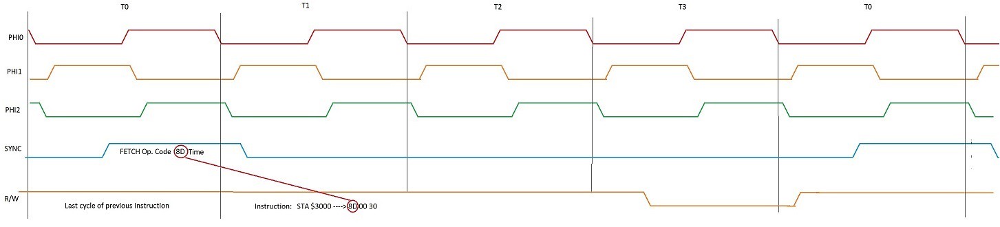
The waveforms seem correct except for one fairly minor detail regarding the clock signals. In your diagram it appears that every change on φ0 is followed shortly thereafter by a change on φ2, which in turn is followed shortly thereafter by a change on φ1. But I believe it should be φ0, φ1, φ2 (not φ0, φ2, φ1).
I'm not sure this detail is documented anywhere. And maybe it doesn't even matter, for what you're doing.

BTW and FYI, nowadays WDC (the only modern manufacturer of 65xx processors) recommends that only one clock pin be used. They recommend you apply the φ2 clock signal to pin 37 and leave pins 3 and 39 unconnected. Also they've changed the pin names slightly, as compared to older NMOS versions of the 6502. The NMOS versions call pin 37 φ0 but WDC doesn't use the term φ0.

-- Jeff

_________________
In 1988 my 65C02 got six new registers and 44 new full-speed instructions!
https://laughtonelectronics.com/Arcana/ ... mmary.html


Top
 Profile  
Reply with quote  
PostPosted: Wed Sep 28, 2022 7:27 pm 
Offline

Joined: Fri Apr 15, 2022 1:56 pm
Posts: 45
Location: San Antonio, TX, USA
Dr Jefyll wrote:
In your diagram it appears that every change on φ0 is followed shortly thereafter by a change on φ2, which in turn is followed shortly thereafter by a change on φ1. But I believe it should be φ0, φ1, φ2 (not φ0, φ2, φ1).
φ1 and φ2 are designed to have non-overlapping high periods (as shown in this diagram) which I think means the order of transition of φ1 and φ2 relative to φ0 necessarily depends on whether we're considering the positive-going or negative-going edge of φ0. I'm not sure if the diagram is strictly correct in this regard but I don't think the order of transitions rules that out. Agreed φ1 and φ2 aren't that relevant for OP's purpose of understanding the cycle-by-cycle activity of instruction execution.


Top
 Profile  
Reply with quote  
PostPosted: Wed Sep 28, 2022 9:39 pm 
Offline
User avatar

Joined: Fri Dec 11, 2009 3:50 pm
Posts: 3354
Location: Ontario, Canada
pjdennis wrote:
I think means the order of transition of φ1 and φ2 relative to φ0 necessarily depends on whether we're considering the positive-going or negative-going edge of φ0.
Thanks. I was too hasty. I only had a close look at the very first edge.

-- Jeff

_________________
In 1988 my 65C02 got six new registers and 44 new full-speed instructions!
https://laughtonelectronics.com/Arcana/ ... mmary.html


Top
 Profile  
Reply with quote  
Display posts from previous:  Sort by  
Post new topic Reply to topic  [ 6 posts ] 

All times are UTC


Who is online

Users browsing this forum: BigEd and 5 guests


You cannot post new topics in this forum
You cannot reply to topics in this forum
You cannot edit your posts in this forum
You cannot delete your posts in this forum
You cannot post attachments in this forum

Search for:
Jump to: