6502.org Forum  Projects  Code  Documents  Tools  Forum
It is currently Tue May 14, 2024 12:24 am

All times are UTC


Post new topic Reply to topic  [ 9 posts ] 
Author Message
PostPosted: Fri Sep 17, 2021 4:27 pm 
Offline

Joined: Sun May 30, 2021 2:16 am
Posts: 374
This is the second entry pertinent to this thread: http://forum.6502.org/viewtopic.php?f=1&t=6777

So I had some time, and I implemented a design using this, from BigDumbDinosaur, for decoding read and write: http://forum.6502.org/viewtopic.php?f=1&t=6777#p87016

I implemented this in one 74AC00.
https://photos.google.com/u/2/share/AF1QipM1BPMjKumR_siFSWqlkTik-T303uN3s1Gt12JGhWNUjX1JeWQdzOpDRnCW4SYbyQ/photo/AF1QipN0xcydyFm9X3VHGuV41eXBMBVDttAs79Z-bFrf?key=MEEyV0kxR1JZT0xkVklickNfR19jZFRMZmxFOERn

I used Dr. Jefyll's connection scheme: http://forum.6502.org/viewtopic.php?f=1&t=6777#p87025

It goes through a 74AC245: https://photos.google.com/u/2/share/AF1QipM1BPMjKumR_siFSWqlkTik-T303uN3s1Gt12JGhWNUjX1JeWQdzOpDRnCW4SYbyQ/photo/AF1QipMhaaL93r8QUio6OxY-QXh0FYfqKA4Z1yZHxEyo?key=MEEyV0kxR1JZT0xkVklickNfR19jZFRMZmxFOERn

As you guys said, the B side faces the CPU and the A side faces outward to the bus.

Then, I implemented the bank address capture scheme found in the 65c816 data sheet, through a 74HC573: https://photos.google.com/u/2/share/AF1QipM1BPMjKumR_siFSWqlkTik-T303uN3s1Gt12JGhWNUjX1JeWQdzOpDRnCW4SYbyQ/photo/AF1QipPj8f0Ns84LB3bV0qJ7HQzPTrY5j_BKv1Gujbwa?key=MEEyV0kxR1JZT0xkVklickNfR19jZFRMZmxFOERn

Then I ran all the lines (data out from the '245, bank addresses from the '573, addresses from the cpu, and /rd and /wr from the '00) into a CMOD A7 35T (has 512k SRAM): https://photos.google.com/u/2/share/AF1QipM1BPMjKumR_siFSWqlkTik-T303uN3s1Gt12JGhWNUjX1JeWQdzOpDRnCW4SYbyQ/photo/AF1QipNjD_R_5yLNmFslgzT18rOuD_1yS7Axrxqeh26O?key=MEEyV0kxR1JZT0xkVklickNfR19jZFRMZmxFOERn

I was extremely careful with the wiring, testing and retesting with the multimeter as a soldered. I also ran a 4mhz clock into the FPGA for phi2 and a 1.8432mhz into the FPGA for LIV2's soft ACIA.

I tested extensively with my multimeter and logic probe, and I caught one issue, but everything checks out now.

My usual verilog tricks don't seem to work. Even with all those signals generated in hardware, I cannot get it to play nice. Can someone propose a verilog scheme that might work? I'm just trying to hook the cpu signals into the internal SRAM and LIV2's acia for basic testing and verification.

I have the data signals from Port A of the '245.

I have the bank signals from the '573.

I have all the processor signals.

And I have the /rd and /wr from the '00.

Jonathan

PS The specs for the CMOD A7 35T can be found here: https://digilent.com/reference/programmable-logic/cmod-a7/start


Last edited by Jmstein7 on Fri Sep 17, 2021 4:50 pm, edited 3 times in total.

Top
 Profile  
Reply with quote  
PostPosted: Fri Sep 17, 2021 4:38 pm 
Offline

Joined: Sun May 30, 2021 2:16 am
Posts: 374
Here are the images:

Image

Image

Image

Image


Top
 Profile  
Reply with quote  
PostPosted: Fri Sep 17, 2021 4:52 pm 
Offline
User avatar

Joined: Thu Dec 11, 2008 1:28 pm
Posts: 10800
Location: England
First comment I think is that you don't have enough decoupling capacitance. Normally we see one electrolytic where the power is brought to the board, and then a ceramic or tantalum next to each chip.

Next, you need to know that you've built what you've designed. So, with all chips out, and your multimeter in continuity mode, you need to test all the pin-pairs which should be connected, to check that they are connected, and then test all pins against the adjacent pin, to check that they are not shorted (unless they are supposed to be.) This only takes a few seconds per pin.

And then, I think you're looking for a review of what you've designed.

After fixing up the capacitors and performing the circuit checks, put your chips back in, and tell us what you see and what you don't see.


Top
 Profile  
Reply with quote  
PostPosted: Fri Sep 17, 2021 4:57 pm 
Offline

Joined: Sun May 30, 2021 2:16 am
Posts: 374
BigEd wrote:
First comment I think is that you don't have enough decoupling capacitance. Normally we see one electrolytic where the power is brought to the board, and then a ceramic or tantalum next to each chip.

Next, you need to know that you've built what you've designed. So, with all chips out, and your multimeter in continuity mode, you need to test all the pin-pairs which should be connected, to check that they are connected, and then test all pins against the adjacent pin, to check that they are not shorted (unless they are supposed to be.) This only takes a few seconds per pin.

And then, I think you're looking for a review of what you've designed.

After fixing up the capacitors and performing the circuit checks, put your chips back in, and tell us what you see and what you don't see.


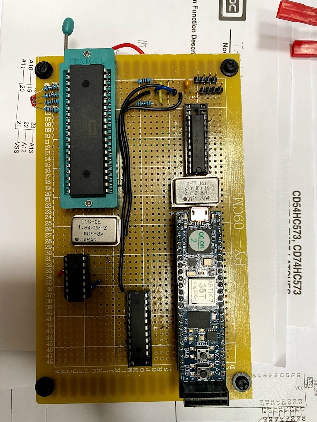
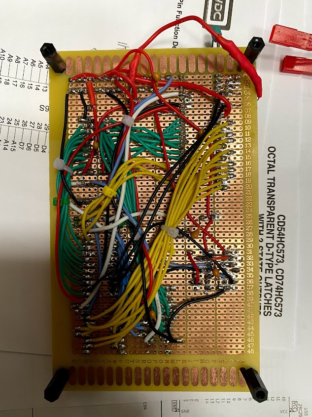
Ed, you’re right, and every chip has a 100nf capacitor. Check the bottom of the board. Also, I checked every connection, for continuity as well, and we’re good. J

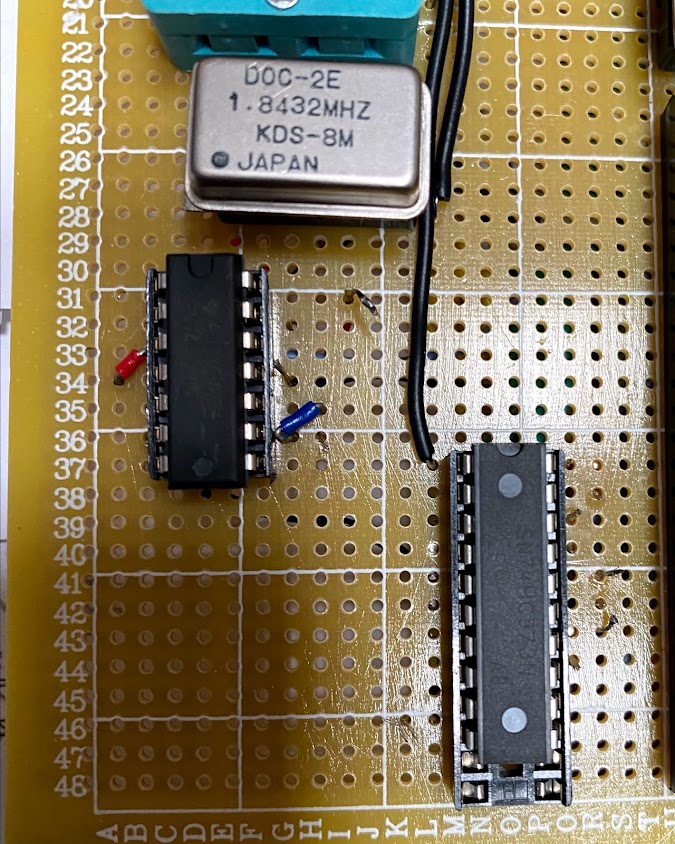
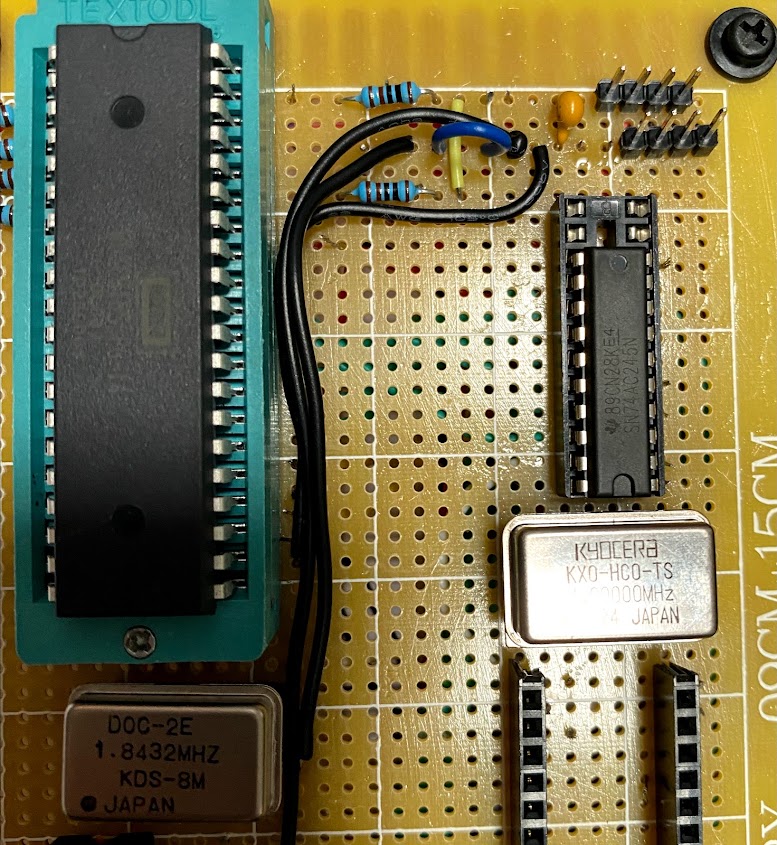
PS do the resistors on the cpu look properly placed?


Top
 Profile  
Reply with quote  
PostPosted: Fri Sep 17, 2021 5:03 pm 
Offline
User avatar

Joined: Thu Dec 11, 2008 1:28 pm
Posts: 10800
Location: England
Good news on the caps.

I notice your 245 is upside down compared to the other chips. That may be as intended, but as a principle of least surprise it's worth placing all chips the same way up.


Top
 Profile  
Reply with quote  
PostPosted: Fri Sep 17, 2021 5:09 pm 
Offline

Joined: Sun May 30, 2021 2:16 am
Posts: 374
BigEd wrote:
Good news on the caps.

I notice your 245 is upside down compared to the other chips. That may be as intended, but as a principle of least surprise it's worth placing all chips the same way up.


Good eye! Yeah, I had to do that to line up Port B with the CPU.


Top
 Profile  
Reply with quote  
PostPosted: Sat Sep 18, 2021 6:37 am 
Offline
User avatar

Joined: Sun Dec 29, 2002 8:56 pm
Posts: 449
Location: Canada
You could use the integrated logic analyzer (ILA) component to dump the signals as the FPGA sees them.
This would show if the address / data is what is expected.
Is block RAM in the FPGA being used as the ROM?

_________________
http://www.finitron.ca


Top
 Profile  
Reply with quote  
PostPosted: Sat Sep 18, 2021 11:34 am 
Offline

Joined: Sun May 30, 2021 2:16 am
Posts: 374
Rob Finch wrote:
You could use the integrated logic analyzer (ILA) component to dump the signals as the FPGA sees them.
This would show if the address / data is what is expected.
Is block RAM in the FPGA being used as the ROM?


Hi, Rob. Thanks for all you're great work (I'm familiar with it).

Anyway, no, I'm using distributed memory, not block. I'm trying to keep everything asynchronous, as much as possible, to match the operation of the 'c816 bus.

I'm using a VIO and single-stepping to test. I don't know how to use the ILA IP core.

Jon


Top
 Profile  
Reply with quote  
PostPosted: Sun Sep 19, 2021 12:17 am 
Offline

Joined: Sun May 30, 2021 2:16 am
Posts: 374
Oh, I probably should have posted this earlier - my code! :oops:

Here it is: https://github.com/jmstein7/65c02-FPGA-with-Acia/tree/main/test_bench.srcs

Sorry!

Jon

Edit: to switch from run mode to diagnostic mode, comment-out the clock module and comment-in the VIO. Do the reverse to go back to run mode. In diagnostic mode, phi2 toggles the clock signal.


Top
 Profile  
Reply with quote  
Display posts from previous:  Sort by  
Post new topic Reply to topic  [ 9 posts ] 

All times are UTC


Who is online

Users browsing this forum: No registered users and 3 guests


You cannot post new topics in this forum
You cannot reply to topics in this forum
You cannot edit your posts in this forum
You cannot delete your posts in this forum
You cannot post attachments in this forum

Search for:
Jump to: