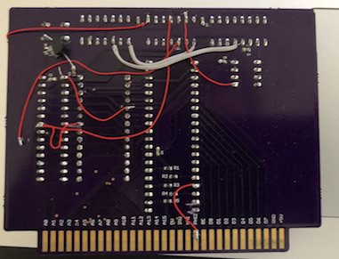
I had always heard to not use the auto-router but after spending 20 minutes routing pins I got frustrated and did it anyway. I mean...looked perfect to me and only took 20 seconds!
Boy was I wrong...
My first mistake was assuming a couple of clicks would replace good old-fashioned manual labor. My second mistake was not checking literally every net and see if they were actually connected.
My third mistake was a typo in one of my labels, missing labels, etc. In my defense, this isn't a project I'm going to submit to NASA. This is just a kick in the pants for me to get more PCB's done. Baby steps.
Anyway, I paid my $24.52 to JLCPCB on Saturday morning (23rd, around 2-3 AM EST) and today, Wednesday 27th (5:30 PM EST) DHL delivered it. My total cost....$24.52 for 10 boards.
Each board is 67.4 mm x 128.3 mm so I didn't qualify for the $2 special. I didn't really try to squeeze my design down. I also got free shipping because it was my first order. I think shipping would have been around $18 or so.
I rip open the package and am immediately impressed with the quality (keep in mind...this is my first). But it feels really sturdy to me. It appears that a seasoned designer could get a pretty good product from them. Although, they do plaster their "makers mark" on it in tiny letters.
I start poking around with my DMM and notice many pins are simply not connected to anything. Upon closer inspection of my PCB layers, I can clearly see they are not connected. My fault. Then again, it was very late at night. lol
Having said all of that...I'm very excited to have received my first PCB. The first one really is the hardest one. I will put a bunch of bodge wires in the back to fix the *many* mistakes I made. I've already started a new design. This design wasn't for a final project. It was a piece of a larger project I'm working on.
All in all, it was a $24 lesson that I can still actually use.
Oh, I guess I could tell you what it is. It's simply a small board that plugs a 65C02, a 62256 RAM and 28256 ROM together with three small "slots". This will allow me to work on glue logic and I/O without constantly wiring those three together.
It has place for a DS1813 and every pin of the 65C02 is brought out to a header. Including the "mystery" pins I've labeled on the board.
Now back to designing!!
