6502.org Forum  Projects  Code  Documents  Tools  Forum
It is currently Sun Nov 24, 2024 1:00 pm

All times are UTC


Post new topic Reply to topic  [ 186 posts ]  Go to page Previous  1, 2, 3, 4, 5, 6, 7 ... 13  Next
Author Message
 Post subject:
PostPosted: Sun Jun 28, 2009 4:06 am 
Offline
User avatar

Joined: Fri Aug 30, 2002 1:09 am
Posts: 8546
Location: Southern California
Here's a repeat of a post I made on Rob Finch's bc_cpu Yahoo forum in June of 2006:
--------------------------
I just got a book offer in the mail for a book called "Microprocessor Design—A Practical Guide from Design Planning to Manufacturing" by Grant McFarland, published in 2006 by McGraw-Hill. 408 pages, ISBN: 0-07-145951-0. I'll put a little more here that's not on the website. The paper that came says on the front:

    Master the basics of microprocessor design the easy way with this hands-on step-by-step guide. Proven microprocessor design crash course keeps your career on the fast track. You get a wealth of tested techniques to help you:

    • Plan for processor design flow and calculate design time and product cost
    • Analyze trade-offs in choosing an instruction set
    • Understand the functional areas of a processor and their impact on performance
    • Construct logic equations required to simulate processor behavior
    • Convert logic design equations into a transistor implementation
    • Produce layout drawings required for fabrication
    • Manufacture integrated circuits
    • Choose the most cost-effective packaging
    • Test and de-bug processors before shipping to customers

The web page above gives the name of each chapter, but here are some more details: (I shortened some things to not have to type so much)

    1. The evolution of the microprocessor
      the transistor
      the IC
      the µP
      Moore's law


    2. computer components
      bus standards
      chipsets
      processor bus
      main memory
      video adapters (graphics cards)
      storage devices
      expansion cards
      peripheral bus
      motherboards
      BIOS
      memory hierarchy

    3. design planning
      processor roadmaps
      design types and design time
      product cost

    4. computer architecture
      instructions
      instruction encoding

    5. microarchitecture
      pipelining
      designing for performance
      measuring performance
      microarchitectural concepts
      life of an instruction

    6. logic design
      overview
      objectives
      intro to hardware description language
      logic minimization

    7. circuit design
      MOSFET behavior
      CMOS logic gates
      sequentials
      circuit checks

    8. layout
      crating layout
      layout density
      layout quality

    9. semiconductor manufacturing
      wafer fab
      layering
      photolithography
      etch
      example CMOS process flow

    10. µP packaging
      package hierarchy
      package design choices
      example assembly flow

    11. silicon debug and test
      design-for-test circuits
      post-silicon validation
      silicon debug
      silicon test

Hopefully it will inspire someone. Doing it in programmable logic would eliminate steps 7 through 10.

[Edited 2/20/18 to update the URL.]
_________________
http://WilsonMinesCo.com/ lots of 6502 resources
The "second front page" is http://wilsonminesco.com/links.html .
What's an additional VIA among friends, anyhow?


Top
 Profile  
Reply with quote  
 Post subject:
PostPosted: Sun Jun 28, 2009 10:05 am 
Online
User avatar

Joined: Thu Dec 11, 2008 1:28 pm
Posts: 10986
Location: England
There's an important activity I'd call 'verification' which shouldn't be underestimated. For a 6502 or close relative that would involve showing that all the instructions act as they should, including response to interrupts, RDY, decimal mode and how they affect the flags. The more complex and more novel the design, the more there is to do in this phase - even minimal pipelining makes it harder.

There's a big advantage in using reconfigurable logic: you can implement early and keep revisiting the design, because you haven't the high costs of tooling and manufacture to deal with.

There's normally also an activity of bringing up a tool chain: an assembler and a monitor in this case, maybe a compiler and debugger in the usual case.

I would recommend an incremental approach: start with a 6502 and then add features and test cases to it. Or, start with a well-understood RISC like ARM or MIPS. If you're looking for a clean and usable successor to 6502, start with a study of existing cores: ARM should be high on that list. If I recall correctly, the increment/decrement addressing modes allow any register to act as a stack pointer, and the conditional execution is a nice approach to short forward branches.


Top
 Profile  
Reply with quote  
PostPosted: Sun Jun 28, 2009 1:59 pm 
Online
User avatar

Joined: Thu Dec 11, 2008 1:28 pm
Posts: 10986
Location: England
Fellow poster Rob Finch has a 6502 core in verilog - see this previous thread which also covered 6502 enhancements.

There's more choice with VHDL: see Sprow's, which derived from Free-ip's 6502, and see also FPGAarcade's version of opencore's T65 (page also links to Peter Wendrich's FPGA-64)

(Looks like the T65 also includes a 65816 core)

For completeness, I also found the M65 in a proprietary HDL.

I just found out that the Cray-1 was clocked at 80MHz, so for me that defines a worthwhile target clock speed!


Top
 Profile  
Reply with quote  
 Post subject:
PostPosted: Tue Jun 30, 2009 9:09 pm 
Offline
User avatar

Joined: Fri Aug 30, 2002 1:09 am
Posts: 8546
Location: Southern California
Quote:
There's an important activity I'd call 'verification' which shouldn't be underestimated

That would fall under #11 above.

Quote:
There's a big advantage in using reconfigurable logic: you can implement early and keep revisiting the design, because you haven't the high costs of tooling and manufacture to deal with

which is why doing it in programmable logic instead of a custom IC would eliminate steps 7 through 10.

Quote:
There's normally also an activity of bringing up a tool chain: an assembler and a monitor in this case, maybe a compiler and debugger in the usual case.

I asked Mike Naberezny about adding a new forum for processor improvements on the forum index (as Tony suggested), and while he didn't mind adding another for a class of topics that would keep coming up, the very fact you mention is why he preferred not to do it at this time—that some of the issues would fall under hardware, some under programming, some under EhBASIC, some under Forth, some under simulation, etc., which are all forums we already have.

Quote:
I would recommend an incremental approach: start with a 6502 and then add features and test cases to it. Or, start with a well-understood RISC like ARM or...

That's basically what I would like to do—start with a 6502 but just extend everything to 32 bits, with not much extra. I should look into ARM, but I still keep hoping to keep it 6502-comfortable.

Thankyou for the links. I had forgotten about the other topic started by Rob Finch himself, to which I made the first reply. Now maybe I can finally get hold of him with the Email address on the web page that appears to be his. I never knew the "bc" in his bc_cpu Yahoo forum stood for "Bird Computer."

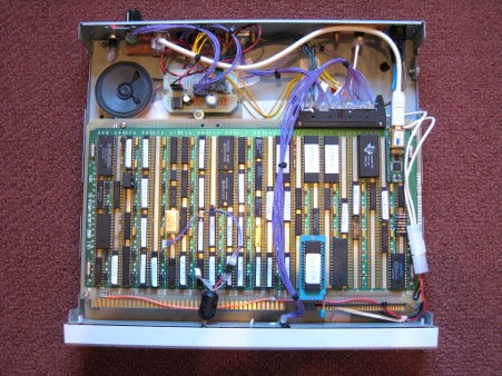
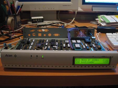
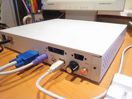
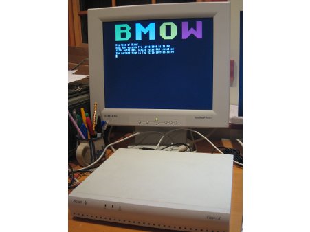
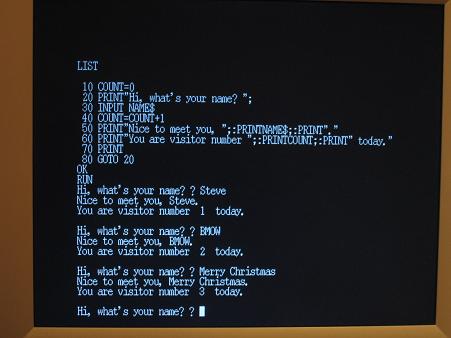
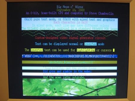
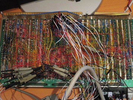
And wow, that BMOW computer you linked is insane! All done in 74xx logic, without a microprocessor. What an accomplishment!


Image Image

Image Image

Image Image

Image Image

Image Image

_________________
http://WilsonMinesCo.com/ lots of 6502 resources
The "second front page" is http://wilsonminesco.com/links.html .
What's an additional VIA among friends, anyhow?


Top
 Profile  
Reply with quote  
 Post subject:
PostPosted: Tue Jun 30, 2009 9:48 pm 
Online
User avatar

Joined: Thu Dec 11, 2008 1:28 pm
Posts: 10986
Location: England
GARTHWILSON wrote:
Quote:
There's an important activity I'd call 'verification' ...

That would fall under #11 above.

Quote:
... using reconfigurable logic: you can implement early and keep revisiting ...

which is why doing it in programmable logic instead of a custom IC would eliminate steps 7 through 10.

Good catch: the missing step 6b isn't missing if it can be deferred.

Thanks for the pictures - well worth another viewing. Inspiring.

Have you come across Randy Hyde's 65C816 Dream Machine essay? I think he was aiming for a 16bit machine which keeps the 6502 philosophy.


Top
 Profile  
Reply with quote  
 Post subject:
PostPosted: Tue Jun 30, 2009 10:02 pm 
Offline

Joined: Fri Jun 27, 2003 8:12 am
Posts: 618
Location: Meadowbrook
I asked Mike Naberezny about adding a new forum for processor improvements on the forum index (as Tony suggested), and while he didn't mind adding another for a class of topics that would keep coming up, the very fact you mention is why he preferred not to do it at this time-- that some of the issues would fall under hardware, some under programming, some under EhBASIC, some under Forth, some under simulation, etc., which are all forums we already have.


When you think about it, such a project requires disciplines and discussions under all the fields. the idea behind a forum group was to address each concern. Perhaps its own Wiki page that has the information added and locked in as it proceeds?

_________________
"My biggest dream in life? Building black plywood Habitrails"


Top
 Profile  
Reply with quote  
PostPosted: Thu Jul 02, 2009 8:16 am 
Online
User avatar

Joined: Thu Dec 11, 2008 1:28 pm
Posts: 10986
Location: England
I've got a couple of suggestions for proceeding without needing a new top-level category:
    - prefix 65Org32-related discussion topics with "65Org32 core" - if they are active topics they will stay together and in any case can be searched.

    - use a topic such as "65Org32 Proposals" and re-edit the posts instead of replying to them. The original poster of each becomes the sole editor, perhaps accepting contributions by private message.

Or, sign up a new project on a site like sourceforge.net, which accepts hardware projects provided they are open source - they will host a wiki, a trac and/or a forum. (I recommend trac very highly as a wiki + issue tracker + task tracker + source code browser.)

It would be good to learn from the experience of the 65gz032 project - I suspect you need one or two highly motivated and productive people to get from a wishlist to a netlist. Pardon the pun.

Cheers
Ed

edit: I see now that the 65gz032 made it to in-circuit testing. Excellent!


Top
 Profile  
Reply with quote  
 Post subject:
PostPosted: Wed Jul 15, 2009 9:53 pm 
Offline

Joined: Thu Jul 26, 2007 4:46 pm
Posts: 105
Warning: This post turned into a bit of a ramble!

I've been mulling over a CPU design of my own for quite a while now. It's definitely not 6502 alike; it's a more "traditional" RISC style load-store register machine, but I think that I can contribute a bit to a 6502 style design based upon my experiences designing it and researching how to design it.

Firstly, a quick description of it: The processor has 32 general purpose registers, named %r0 to %r31. %r0 is hardwired within the processor to be zero, as this has proven quite useful in practice [MIPS also does this]. %r31 is used for the frame pointer; %r30 is the default procedure return address register. The processor has an additional bank of 32 special function registers, which is not full, for controlling the processor and similar purposes.

All instructions are 32-bits and feature seven fields:
3-bit Write control: Contains the WZ (Write Zero), WC (Write Carry) and WR (Write result) flags.
3-bit Condition code: Each instruction can be made conditional on the aforementioned flags.
6-bit Opcode: Self explanatory
4x5-bit: Fields F1 through F4. Can refer to a register or contain a literal, and may be ganged together depending upon the instruction. Inputs generally come from F1, F2 and F3 in that order; Outputs are always determined by F4.

The opcode space is slightly reduced by some instructions which gang the opcode's LSB with the 15-bits of F1, 2 and 3 to form a 16-bit literal.

All operations are 32-bit wide except for loads and stores, which may be 32, 16 or 8 bit wide.

Instructions are decoded using microcode. Microcode need not be slow; in my case most instructions decode in one cycle. Microcode addresses are 7-bit, and the first microinstruction of an instruction is simply it's opcode zero extended. I haven't determined the microinstruction size yet.

A microinstruction simply consists of the various signals that are to be distributed to the various segments of the CPU pipeline, and the next instruction address. For example, the microcode for the add instruction would say the following:
ABus = Reg[F1]
BBus = Reg[F2]
CBus = F3
ALU Operation = Add
Memory Operation = Nop
WriteRegister = Reg[F4]

The instruction
add %r1, %r2, 5, %r3
Would do %r3 = %r1 + %r2 + 5

The next address field contains the address of the next microinstruction in the instruction; the last instruction contains the all-one address, which the microcode sequencer interprets to mean "Instruction finished". When this address is branched to, the sequencer branches to the next instruction's address if no interrupt is waiting (If one is, it branches to the interrupt microcode address - the all-one address)

The pipeline is structured as
Fetch -> Decode -> ALU -> Memory -> Writeback

One feature I'm really fond of is the fixed point support: The multiply and divide instructions contain, respectively, post and pre shift values in F3. This means that, with a 16.16 fixed point value, you can do
MULS %r1, %r2, 16, %r3
or
DIVS %r1, %r2, 16, %3

(Though the first implementation will probably lack a hardware divider)
And get a 16.16 value out. (The ALU operates on 64-bit intermediates)


Top
 Profile  
Reply with quote  
 Post subject:
PostPosted: Thu Jul 16, 2009 11:25 am 
Offline
User avatar

Joined: Tue Mar 02, 2004 8:55 am
Posts: 996
Location: Berkshire, UK
I've been following this discussion for a while and it seems to me that many of the suggestions would lead to processors that would be so different from the 65C02 as to be new devices in their own right.

If you want to extend the 65C02 to 32-bits whilst remaining faithful to its approach and style you will have to follow the same path as the 65C816 and end up with something like the (once proposed) 65C832. This approach maintains architectural and code compatibility into 32-bits.

Once you start changing the instruction set, addressing modes or number of registers you lose this backwards compatibility have effectively have just created a new processor family. The 65GZ032 is good example of this. While it offers a 6502 compatibility mode its native 32-bit mode is very different and almost unrecognizable as a 6502 derivative.

If you want a 32-bit RISC based CPU then there are plenty of good commercially available devices. Do we really need to design yet another?

If we want a 32-bit 6502 then I'd suggest we implement a 65C832 in RTL or emulate within another micro-controller at low speed on a carrier board that fits a 65C816 socket.

Just my $0.02

_________________
Andrew Jacobs
6502 & PIC Stuff - http://www.obelisk.me.uk/
Cross-Platform 6502/65C02/65816 Macro Assembler - http://www.obelisk.me.uk/dev65/
Open Source Projects - https://github.com/andrew-jacobs


Top
 Profile  
Reply with quote  
 Post subject:
PostPosted: Fri Jul 17, 2009 4:05 am 
Offline
User avatar

Joined: Fri Aug 30, 2002 1:09 am
Posts: 8546
Location: Southern California
bitwise, although VBR started the topic, he has said little since then and hasn't complained about any of my ideas, so let me present the "Reader's Digest" version of my proposal, because it is very much a 6502 (with the extra 65816 capabilities), just completely 32-bit. Basically a byte just becomes 32 bits instead of 8.
  • Not a RISC. Same Von Neuman architecture as 6502. Op code and operand are not combined. Most instructions remain the same, unlike the 65GZ032.
  • Has 6502's A, X, Y, S, P, and PC registers, and 65816's DP, DB, and PB registers-- but they're all 32-bit (although only about 8 status register bits would get used.)
  • Simpler, because everything is in ZP (or, more accurately, DP), because ZP has over 4 billion addresses. No operand requires more than one fetch. Even the 65816's bank boundaries are gone.
  • Since the data bus is 32-bit, there will not be separate 8-, 16-, and 32-bit modes like the 65832 had.
The what-about's are addressed in earlier posts, like that 32-bit-only is not a problem for 8-bit I/O ASCII data.

It would not have an emulation mode to run old 6502 code directly, but your programming and construction knowledge does transfer directly. There's almost nothing new to learn.

Trying to emulate one with a microcontroller with nearly 80 I/O pins (10 8-bit ports) would be extremely slow, like having phase 2 be a few tens of kHz; so that's out of the question.

I'll try to post some code examples later.

_________________
http://WilsonMinesCo.com/ lots of 6502 resources
The "second front page" is http://wilsonminesco.com/links.html .
What's an additional VIA among friends, anyhow?


Top
 Profile  
Reply with quote  
 Post subject:
PostPosted: Fri Jul 17, 2009 10:05 am 
Offline

Joined: Thu Jul 26, 2007 4:46 pm
Posts: 105
I still don't understand why you want to go for a word addressed architecture over a byte addressed one. With a byte addressed architecture, you just need one opcode for each sized load (Or flags somewhere indicating the load size), and a bit of logic somewhere to zero/sign extend values.

A major problem I can see for you though is opcode alignment. If instructions are 8-bits, and followed by a 32-bit literal, then most of the time the literal is going to be unaligned and you're going to be spinning for at least a couple of cycles loading it.

If you want to avoid that kind of delay, you need a prefetch buffer or such; of course, now were heading into a pipelined architecture. Admittedly, pipelining isn't that much more complex than not pipelining. The main problem is interlocks to ensure an instruction doesn't enter the pipeline before one it's dependent upon finishes, and duplication of functionality in different stages (The second is more an issue with CISC style architectures - the RISC one I'm designing doesn't really have this issue).


Top
 Profile  
Reply with quote  
 Post subject:
PostPosted: Fri Jul 17, 2009 10:41 am 
Online
User avatar

Joined: Thu Dec 11, 2008 1:28 pm
Posts: 10986
Location: England
I read a little about coldfire the other day: it seems it was a simplification of the 68k, which allowed for smaller faster implementation. Worth a look. They chose to go for variable-length instructions, for the sake of code density.

But I think the 32-bit byte idea here will have every fetch, and therefore the opcodes, be 32 bits. The number of memory accesses will be very like the 6502's, with the extra width being useful for a proportion of the time.

In the interest of simplicity, and similarity with 6502, memory and pincount are being thrown in.

(I suspect there would need to be a sign-extend for the case where a fetch accesses some 8-bit-wide data which is to be handled as signed.)

Of course a 32-bit opcode does allow for embedded operands and easy decode: increment can be extended into an add short literal for example. It would be possible to add 16-bit relative branching, maybe even 24-bit relative, but I think the idea would be not to do that: a 32-bit branch opcode followed by a 32-bit offset.


Top
 Profile  
Reply with quote  
 Post subject:
PostPosted: Fri Jul 17, 2009 7:06 pm 
Offline
User avatar

Joined: Fri Aug 30, 2002 1:09 am
Posts: 8546
Location: Southern California
.
Ed's got it. There are no alignment problems. On the 6502, ADC# takes two bytes and two clocks for any operand up to $FF. On the 65Org32, it takes two bytes (although they'll be 32-bit ones) and two clocks for any operand up to $FFFFFFFF.

It's true that many of the bits in the op code are not strictly needed, but the 6502 simplicity is kept, and I suspect that the wider op code field could simplify the instruction-decoding logic. It does however allow for some BBS/BBR/SMB/RMB-type instructions like the Rockwell and WDC 65c02's have where one of the operands is integrated with the op code, for limited use like an op code to shift left 22 bits with the barrel shifter instead of having to do ASL 22 times (or whatever number you need).

I've dealt with I/O that was 4-bit and even 1-bit with an 8-bit 6502 and there of course no problems with alignment or anything else. There are different ways to handle the rare sign-extension need that Ed mentions, but even though most of my 6502 programming is in Forth which routinely handles 16-bit cells, I don't remember ever having to extend the sign of an 8-bit number to a 16-bit one. 16- to 32-bit yes, but not very often. The Forth word S>D (single to double) does that.

When I program embedded controllers (and I've brought quite a few to market), 8-bit is really enough. And to run 6502 code, I will continue to use a 6502, so I don't need the bigger processor to have an emulation mode. Many on this forum don't get heavily enough into this kind of work to justify going to 32-bit, and that's ok; but it would open up a lot possibilities for my workbench computer that are more math-intensive and keep larger amounts of data while keeping the simplicity of the 6502.

_________________
http://WilsonMinesCo.com/ lots of 6502 resources
The "second front page" is http://wilsonminesco.com/links.html .
What's an additional VIA among friends, anyhow?


Top
 Profile  
Reply with quote  
 Post subject:
PostPosted: Sat Jul 18, 2009 1:03 am 
Offline

Joined: Thu Jul 26, 2007 4:46 pm
Posts: 105
It must be just me who feels that wasting 3/8ths of your code space is, well, wasteful.

The other thing is not supporting byte accesses is going to make porting software a nightmare. Much assumes that you can address stuff bytewise.

Even if leaving your instructions 32-bit wide, I see no reason for not implementing bytewise access. It will vastly simplify any string handling. And it's not that complex; a small amount of logic in the memory unit for zero and sign extending values, and for telling the bus how big an access your doing. Thats it. And with 24 otherwise wasted opcode bits, why not do it?! You can leave the registers 32-bit, and just let programs ignore the upper portions.


Top
 Profile  
Reply with quote  
 Post subject:
PostPosted: Mon Jul 20, 2009 3:42 am 
Offline

Joined: Sun Jul 19, 2009 9:24 pm
Posts: 13
I just registered, but I have some ideas as well, many of them from some RISC processors. I am not proposing a RISC processor however because that's not what a 65xxx is anyway. It is possible that some think my ideas don't retain the spirit of 65xxx processors but I think they definitely do, while improving it at the same time. This is not a finished plan and probably contains some errors or stupidities. I don't propose anything like deep pipelining, out-of-order execution or large caches that make desktop processors so complicated nowadays, as this processor should fit in a FPGA. Constructive criticism is excepted and welcome :)

Here comes:

- First of all, processor would be 32-bit internally as far as registers are concerned, but data bus would be 16 bits for ease of implementation (and fewer pins would be required as well). I will explain "ease of implementation" shortly.

- There would be two accumulators, A and B, like in 6809. There would be four index registers, X, Y, Z and SP. Everything 32-bit, of course. I believe this would improve support for high-level languages and also make machine language programming easier. Address space should be flat and any banking is to be avoided.

- All instructions would be either 16-bit or 32-bit (maybe 48 bits in some cases) in length, with a 16-bit opcode and possibly a 16-bit (or 32-bit) data word. This combined with a 16-bit data bus would ensure there wouldn't be unaligned instructions, ever. Large constants could be put in a table or loaded with several instructions (LDA.W #HIWORD; ASLA #16; ORA.W #LOWORD) and index registers could be used for address calculations, but to ease machine language programming some 32-bit absolute/immediate instructions could be provided. None of those instructions should be needed in principle though.

- There should be 8-bit, 16-bit and 32-bit load/store instructions with separate opcodes. This also applies to instructions between an accumulator and a memory location.

- There would be ADQ (ADd Quick) that would replace INC/DEC and fit in 16 bits, like in 680x0. The range could be +/-8, covering all common indexing cases and being more powerful than double INC/DEC as proposed earlier.

- As there are 65536 opcodes available and maybe about 256 needed, there could be an optional conditional execution for every instruction, like in ARM. This could be used to eliminate branches over few instructions and would be zero-cost. There should still be enough space to encode shift counts etc. to an 16-bit opcode.

- Fast divide/multiply instructions would be provided if feasible. Floating point wouldn't be supported, except maybe by a separate co-processor.

- There could be a few IRQ vectors/lines as well, to make interrupts faster.

Putting on the asbestos suit..


Top
 Profile  
Reply with quote  
Display posts from previous:  Sort by  
Post new topic Reply to topic  [ 186 posts ]  Go to page Previous  1, 2, 3, 4, 5, 6, 7 ... 13  Next

All times are UTC


Who is online

Users browsing this forum: No registered users and 8 guests


You cannot post new topics in this forum
You cannot reply to topics in this forum
You cannot edit your posts in this forum
You cannot delete your posts in this forum
You cannot post attachments in this forum

Search for:
Jump to: