BigDumbDinosaur wrote:
As I earlier posted, I really haven't given this much thought. However, I am of the opinion that an expansion bus should be fully isolated and buffered from the MPU's buses and that the isolation/buffer hardware should mediate all transfers. Incidentally, bringing signals such as /IRQ, RDY, VDA, etc., out to the bus is still effectively taking the MPU's buses off-board. The expansion bus' "slots" shouldn't know about signals like that, and should be driving an interrupt encoder rather than directly accessing /IRQ or /NMI. Signals such as BE, RDY and VDA are MPU bus management signals, and should be confined to the mainboard circuitry only.
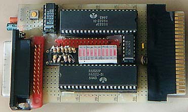
Look at the PCI bus for answers. It doesn't have to be as complicated as PCI, but should try to adopt some PCI features. This may be a good application for some 65C22s to act as bus drivers.
Hi BDD,
This goes a bit against what I'm after. Such a bus would need a lot of additional programming to use and that kind of beats the primary intent - to define something that makes it real simple to make cards for and to keep the programming as light as possible.
As far as interrupt control, that's something the auxiliary lines could be used for. A user that requires more sophistication for an interrupt driven system can use those lines so that the interrupting device can place a code into an interrupt register on the CPU card when it asserts /IRQ or /NMI. The first part of the interrupt routine would be to check that register. This would allow 'smart' devices the opportunity to define multiple interrupts. Or they could be used to facilitate 'slot' based interrupts or something even more sophisticated.
All that said, I can see the attraction of an arbitrated asynchronous bus for peripherals. Especially in systems where it is desirable for the CPU to run as fast as possible. So maybe there is room here for two bus structures. One that is simple, flexible and a bit unsophisticated, another more performance oriented that separates the CPU and memory on a faster, synchronous bus supporting maximum processor speed and multiple concurrent processes while keeping the peripherals on an arbitrated asynchronous bus that is more rigorously defined.